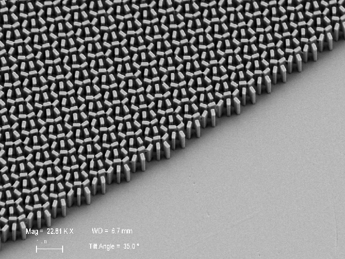
The metalens uses patterns of microscopic pillars to redirect and focus light. Courtesy of John A. Paulson School of Engineering and Applied Sciences.
Engineers at Harvard University have published their proposal for a large area lens design that addresses the high-demand of the technological age. With a nod to Moore’s Law, they sought to unify two separate industries: lens-making and semiconductor manufacturing. Their solution, the metalens, answers the question “What if we made lenses the same way we manufacture computer chips?”
The Concept of Metalens
Replacing stacks of standard glass lenses with a single, large area wafer-thin metalens could have important implications on the modern optical industry. Cameras, telescopes, and other imaging systems could shrink drastically in size without compromising image quality.
The key to mass-production of lenses is the metasurface. These microscopically engineered sheets control light with arrays of optical elements. The subwavelength features create a pattern on the chosen surface to induce variation in phase, amplitude, and polarization. Photolithography techniques would allow manufacturers to tailor the properties of each feature to control the transmission, reflection, and scattering of light with the ease associated with microchip fabrication. Whereas traditional lenses use the curve of glass to focus light, metalenses use these so-called pillars to bend wavefronts toward a focal point.
The Harvard team details the entire model for their metalens from design to mass-manufacturing potential in Optics Express. Their objective: to “demonstrate large area metasurface optics using a process that could scale to high volumes and low costs.”

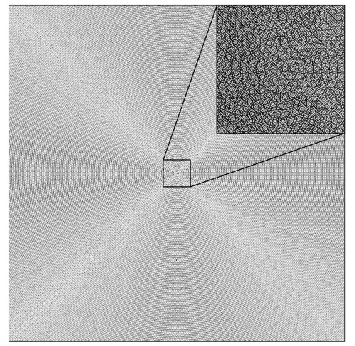
The above image provides perspective into the complexity of a metalens pattern. Courtesy of Optics Express.
The Design of the Metalens
The entailed metalens consists of a four-inch silica wafer covered in patterns of microscopic silicon pillars. Herein is the first challenge in creating a large area metalens because transcribing millions or billions of pillars onto a macroscopic face creates unmanageably high data density. The Harvard team, however, implements a compression algorithm that cuts the required file size by several orders of magnitude. Additional details on this algorithm are outlined in their paper.

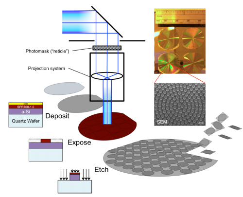
This image depicts the quick and fairly straightforward method to mass produce metalenses. Courtesy of Optics Express.q3
Fabrication of the Metalens
The team uses existing photolithographic technology to produce their metalenses. This allows for manufacturers to mass produce the devices with the same precision and efficiency as IC chips.
A simple outline of the process includes first depositing the silicon film and then photoresist onto a wafer. The layered system is then repeatedly exposed to a projected pattern and UV light while the wafer shifts position. The pattern can then be etched into the silicon to complete the metalens. This method of photolithographic “stepping” can produce hundreds of wafers per hour.

Above is an image taken during experimentation with the large area metalens. Courtesy of Optics Express.
The Result
The rapid and relatively simple process does not sacrifice quality. The team analyzed the imaging capabilities of their metalens using a simple horizontal microscope. Their findings show a high focusing efficiency of about 92%, minimal chromatic aberration due to low NA, and no spherical aberration due to the flat surface of the lens.
In addition, at only 600 nanometers wide, the metalens is a very close approximation for the ideal thin lens equation. While this equation is common in many introductory optics courses, we rarely see these measurements in experimental practice.
Manufacturing Implications
Metalenses are extremely thin, high-quality, and cost-effective.
The Harvard group envisions an industry where optical and electronic parts are produced with the same equipment in the same place. Photolithgraphic stepping is already common practice in many facilities, allowing for simple integration. Manufacturers could imprint optical shaping patterns in mere milliseconds.
Metalenses fit perfectly in a tech industry driven by Moore’s Law. This proposal provides a clear path toward mass-production. Telescopes, cameras, and smartphones will continue to improve in quality while also becoming more convenient, smaller, and cheaper. The metalens could one day render bulky glass lenses obsolete.
For more information on the first large area metalens, you can find the paper here.
