Silicon photonics is the technology of using optical processing components made of silicon itself, rather than other materials. Electronic interconnects with copper contribute to high power consumption and bandwidth limitations, further restricting Moore’s law. Using silicon optical interconnects solves this problem by having low losses and higher bandwidths. With the industry’s well established silicon manufacturing processes, companies such as Intel, IBM, and Luxtera are working to produce faster photonic circuits with existing silicon manufacturing processes.
Silicon is a poor emitter of light as it has an indirect band gap. This has made direct band gap III-V semiconductors to dominate optical devices rather than silicon. They have been used to design quantum well lasers that can be modulated to feed data into optical fibers for data communication. However, design with these materials comes with the cost of lower yield efficiency, and different fabrication processes. Also, interfaces of these components with silicon electronic circuits are necessary. Silicon photonics (SiPh) can avoid these problems by keeping all components in the optical domain, while maintaining low losses and high bandwidths. This can dramatically reduce the cost of production and still use standard silicon foundries.
Optical interconnects
Interconnects are necessary for relaying information between different components in a circuit. Copper is the preferred interconnect for electronic circuits. However, silicon can transmit data faster with lower losses, if operated in the optical domain of around 1550 nm. Silicon photonic circuits are designed to manipulate light around this window. In the past, this change did not offer significant improvements in speed, because the optical signals were still required to be converted into electrical signals for processing. This step is time consuming. Building processing components such as electro-optic modulators in silicon instead removes intermediate electronics. Applications include developing fast interconnects and high-bandwidth optical switches for speeds upto 100G to 200G for connections in datacenters. Companies such as Intel are currently working on bringing SiPh circuits to the market to move from 4G to 5G networks.
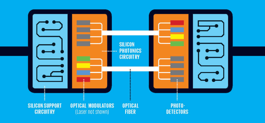
Silicon photonic components for faster interfaces with fiber optic links and electronic circuitry. Courtesy of IEEE Spectrum
Silicon on Insulator (SOI)
Silicon on Insulator (SOI) technology is used to fabricate photonic chips. The components are fabricated by first depositing an insulator layer such as silicon dioxide, over which a layer of silicon is deposited and patterned. The image below shows a silicon rectangular waveguide deposited over a silicon dioxide insulator. Patterning can be done using electron-beam lithography.
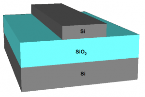
Silicon rectangular waveguide on top of a silicon dioxide insulator. Courtesy of NanoSOI
Components such as filters, sensors, and electro-optic modulators are all patterned on the silicon overlayer. The size of the structures are in the order of micrometers as the region of operation is in the infrared region (1.5 um).
Silicon photonic components
Resonators and filters:
Waveguides and resonators can be made using SOI technology. Light can be guided when it is coupled at the input of a rectangular waveguide. Ring resonators are built by designing a loop of specific length. The resonant frequencies occur when the wavelength is integer multiples of the total length. Such resonators can be built in silicon with radii smaller than 1 um. For example, they can be used to build filters, sensors and electro-optic modulators. The image below shows a notch filter designed using a silicon ring resonator.
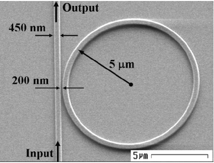
Ring resonator designed to control the output of a nearby waveguide. Courtesy of OSA.
Filters are designed by coupling light from a waveguide into the ring resonator. The coupling is controlled by the distance between the ring resonator and the main waveguide. When the guided light has a frequency close to the resonant frequency of the ring resonator, the light is coupled into the ring resonator efficiently. The output intensity in the waveguide is reduced as a result. This can be used to design an on-chip notch filter that detects a particular frequency.
Sensors:
The same topology can be used to build sensors to detect certain bio-molecules. The image below shows the change in the light output when certain protein molecules bind to receptors on the ring resonator.
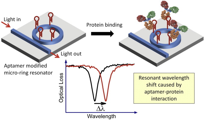
Sensors to detect molecules designed using ring resonators. Courtesy of ScienceDirect.
On-chip sensors can be built if some analyte changes the refractive index of a medium. The adsorbed molecules change the refractive index of silicon. This shifts the resonant frequency in the ring resonator, which can be detected as a change in output power.
Electro-optic modulators:
Non-linear effects can also be used to modulate the refractive index of silicon, which can be detected. Pockel’s effect can be used to change the refractive index of silicon with applied voltage. The structure looks slightly different, with doped silicon used to create p-i-n junctions. Metal contacts are added on top to change the voltage across the ring resonator. This can be used to build an electro-optic modulator as shown below.
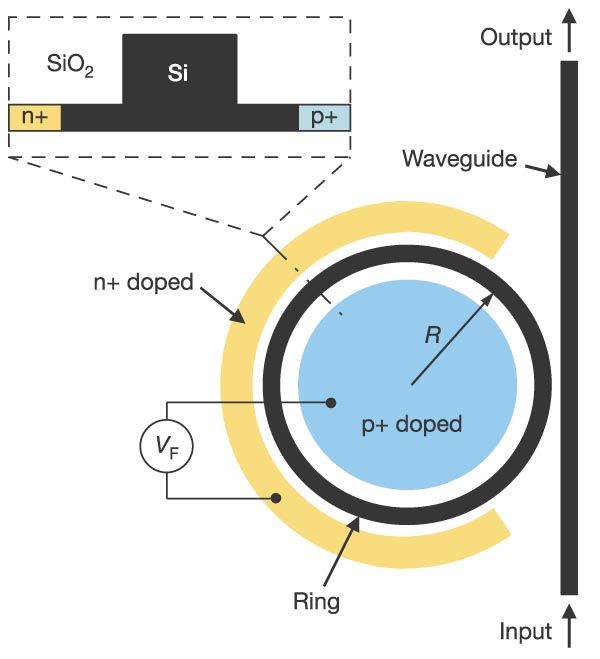
Electro-optic modulator using doped ring resonator. Applied voltage can modulate the output. Courtesy of Nature.
The ring resonator is sandwiched between p and n doped regions. Applying a voltage difference between them developed an electric field in the silicon ring. By Pockel’s effect, there is a change in the refractive index of silicon, which changes the wavelength of light coupled into the ring. This wavelength is modulated with applied voltage.
While silicon photonics does offer the promise of all optical processing elements, not having laser components in silicon can be a limitation. Intel’s design of a silicon Raman laser counters this problem. Moreover, hybrid silicon schemes with InP are also being explored.
Check out Findlight’s collection of electro-optic modulators, integrated laser components, and non-linear crystals for using optical processing elements in your designs.
