Imaging tools help us see into the world that is not possible with our naked eyes. It was with the invention of the microscope and the telescope that big frontiers in science were reached. We unlocked the ability to look into distant planets, and discover that diseases could be caused by microscopic bacteria. Charge Coupled Devices (CCD) and CMOS sensors provide excellent image quality for applications ranging from medicine, to industry, and scientific research. CCD cameras can be used in spectroscopy and even in very sensitive measurements required in outer space. In today’s blog post, we will discuss the properties of these devices and compare their performance parameters.
Charged Coupled Devices (CCD)
CCD devices are layered constructs designed in such a way that they collect incoming light energy when a high voltage is applied. There are four layers in a typical CCD device: the bottom silicon substrate doped with boron, a channel stop layer, an oxide layer, and a gate electrode for control. When the gate voltage is high, a potential energy well is created below the oxide layer. The incoming photons can excite electrons in the potential well, which can be collected and directed. The surrounding doped region prevents the excited electrons from leaking out. The image below shows the various layers with the potential well formation. Typically 10,000 to 500,000 electrons can be collected in such a potential well.
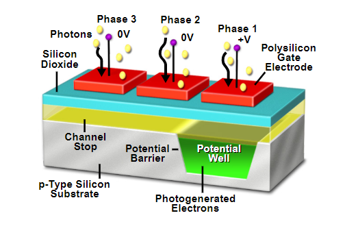
Structure of charge coupled devices. Image courtesy of MicroscopyU.
The collected charges are then shuttled to nearby wells by changing the voltages one after the other. This way the detected charges can be transferred for analysis. Because of the voltage control of the potential wells, the electrons only follow in a particular path with 99% efficiency from detection to analysis.
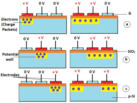
Shuttling charges from detection for analysis by changing voltages. Image courtesy of Elprocus.
Spectral Response of a Typical CCD
Factors that should be considered while choosing charge coupled devices for an application are the pixel size, array size, dark noise, speed, quantum efficiency, full-well capacity, and spectral response. The pixel size for CCD devices is between 6 and 25 micrometers. The array size is determined by the number of rectangular pixels and the dimensions. For example, a phone camera comes with approximately a million pixels, while large cameras could contain as much as several billion pixels. The next factor to consider is the speed, which is limited by the speed at which the charges can be transported from the detected well to the analysis well. The full-well capacity can be as much as 500,000 electrons or more depending on the applications. Dark noise in measurements can occur due to heat, which can be minimized by keeping the device cool.
Spectral response also determines the range of frequencies that can be detected with a CCD device. Detection with Silicon CCD devices is possible from 400-900 nm with high quantum efficiency. For UV detection, the CCD devices can be modified to enable imaging.
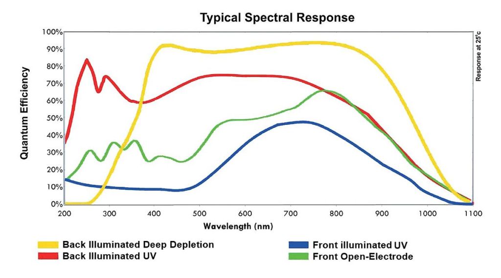
Spectral response of CCD devices. Image courtesy of Horiba Scientific
Color Images from CCD Cameras
A simple CCD camera absorbs all the colors if it is exposed to various colors, but only detects the intensity of incoming light. To modify the device to create color images, a Bayer filter was invented in 1976. This filter has units which let only red, green or blue light through. By selectively letting different colors in a particular region, color images can be produced. Bayer filter is used in most phone cameras.
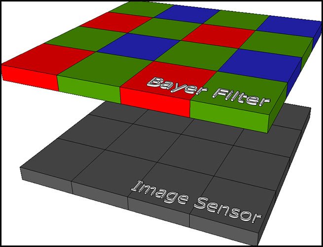
Bayer filer over an image sensor can help create color images. Image courtesy of DIY Photography.
CMOS Sensors
CMOS Imaging only involves a photodiode and, thus, is easier to analyze. The structure consists of a microlens array focusing the incoming light onto a photodiode. The current response from the photodiode is proportional to the intensity of the incoming light and thus can be used to make less precise sensors than CCD devices. We have discussed the uses and the functions of a photodiode in a prior blog post.
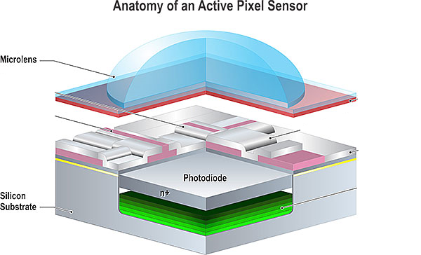
Structure of a photodiode based CMOS imaging sensor. Courtesy imaging-resource.
Comparing CCD and CMOS
CMOS imaging, also referred to as active pixel sensors, consists of photo diodes connected to a CMOS amplifier to detect the signal. The device can be manufactured at a relatively low cost and integrated into standard semiconductor assembly line. For charge coupled devices, a high precision requires careful control of the device parameters to optimize for various applications. For example, CCD cameras for space imaging are designed to resolve low number of photons as there is only weak light coming in from distant stars.
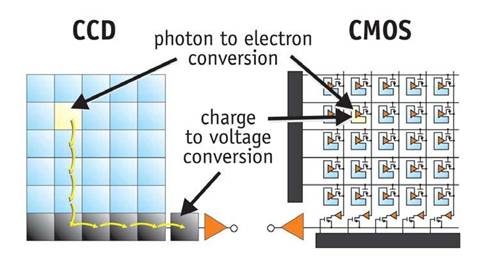
Difference in layout of CMOS and CCD devices. Image courtesy of DifferenceBetween.
The detection speed is faster in a CMOS sensor as there is no shuttle of charged required. The noise however is higher and also the quantum efficiency in these devices are usually between 15-35% compared to 25-95% in charge coupled devices. The table below compares the advantages for various parameters.
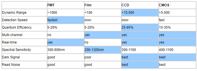
Characteristics of CCD and CMOS devices compared. Image courtesy of specinst.
Medical Imaging
Medical imaging done using fluorescence emits light in the visible region. Visible region is well within the detection range of charge coupled devices and can thus be used to form sharp color images of biological samples. For example, blood arteries images using confocal microscopy is shown in the image below.
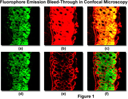
CCD imaging from confocal microscopy of blood vessels. Image courtesy of Olympus Lifescience
With diode lasers being designed in the UV and visible region using nitride materials, fluorescence spectroscopy can be done with compact laser setups with laser diodes and fiber optics rather than table-top solid state lasers. Moreover new nanoparticles acting as fluorescent dyes opens up a wide range of biological molecules and species that can be imaged, which makes it an exciting field. CCD cameras can be used here to capture high resolution images of these samples.
Are you looking for CCD or CMOS based cameras? Check out FindLight’s vast collection of products for various camera solutions including
Did you like the article? If you did, please share. You might also enjoy our Essential Guide to Streak Cameras.
