Photoelectronic devices combine the vast use of electronics for processing information with the detection and the manipulation of light. Devices such as photodiodes are useful for detecting incoming light of various intensities and wavelengths. They can be integrated with electronic circuits to create versatile light sensors. Photodiodes have also been used for information processing to detect information sent through optical fibers for long-distance communication. Recently, nanostructure photodiodes have been shown to reduce error in measurements and capture more light during detection. In this article we will discuss the various properties and applications of photoelectronic devices.
Structure and Operation of Photoelectronic Devices
Photodiodes are built using doped semiconductor materials forming junctions. Light is typically targeted at the junction region. Here the incoming photon excites an electron from the valence band to the conduction band in the material, leaving behind a hole in the valence band. The newly formed electron-hole pair drift to opposite sides by an existing electric field at the junction, before they can recombine. Many ways exist to increase the efficiency of this drift process. These different ways are used to make more efficient photodiodes such as avalanche diodes, pin diodes and nanowire photodiodes.
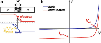
Structure, characteristics, and band diagram in a typical photodiode. a) Device structure and band diagram. b) Current-Voltage characteristics. Courtesy of Springer
Photodiodes have an applied bias voltage to increase detection efficiency. Reverse bias is applied to increase the electric field in the junction region so that the electrons and holes are swept away from the junction. The parameters of interest for a photodiode are its response sensitivity, response time, and dark current. Response sensitivity refers to the amount of electrons generated from a single photon. Response time refers to the time taken to generate the current. Diodes always have a small saturation current during reverse bias. This is referred to as the dark current as it always exists and is not generated by the incoming light.
Avalanche Photodiodes
Avalanche photodiodes create many electrons from a single photon. Similar to a mountain avalanche where a rolling stone can gather more speed and mass with gravity, the electrons increase in number with electric field. If the reverse bias voltage is increased tremendously and is close to the breakdown voltage of the diode, avalanche breakdown can occur. Under this process, high reverse bias induces a very strong electric field in the depletion region. This causes the electrons to pick up enough energy to knock out an electron from the device, which knocks out further electrons. Through this process, a chain reaction occurs where many electrons are created by a single photon. The image below illustrated the multiplication of carriers at the junction during avalanche breakdown.
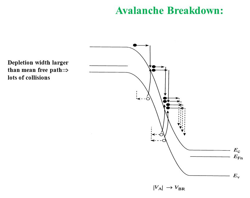
A single excited electron can trigger emission of many electrons under high electric field. Courtesy of COMSATS
The principle is similar to the operation of a photomultiplier tube. While photomultiplier tubes are bulky, semiconductor APDs offer smaller form factors and are suitable for compact light detection devices. The image below shows the generation and flow of charges when integrated with a simple circuit with a battery.
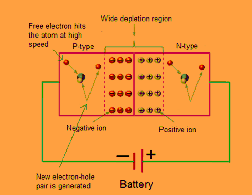
Circuit shows design of an avalanche photodiode circuit, with the current knocking out more carriers along the way. Courtesy of Elprocus
PIN Photodiodes
PIN diodes are a slight modification of p-n junctions where there is a long intrinsic region in between the p-type and n-type regions. The main feature of the middle intrinsic region is that is has an electric field drop across it. The electric field helps facilitate transport from the middle section to the outer sections faster. The image below shows how such carriers can be swept from the intrinsic region.
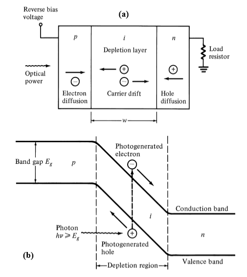
Regions in a p-i-n photodiode. Courtesy of ResearchGate
PIN diodes are also used as fast radio-frequency modulators for this reason. The electric field in the intrinsic region causes fast movement of carriers, thus increasing the frequency at which these devices can respond.
Photovoltaics and Nanowire Photodetectors
In contrast to photodetectors where an external reverse bias voltage is applied to detect the current, there is no bias voltage applied for photovoltaic devices. This is because the light is forced to sweep away carriers from the junction region to develop a voltage across the junction. Photovoltaic cells convert light energy into electrical energy for storage.
Many techniques have been made to increase the amount of light that is converted to electrons. Anti-reflection coating reduce the amount of reflected light. However, nanowire arrays are better than anti-reflection coatings in absorbing light serving as promising candidates for the future. Nanowires increase the efficiency of absorption by two factors. The first factor is the enormous increase in the junction surface area causing more absorption of light to occur. The second factor is related to the physical structure of these constructs as the reflected light has a high probability of being reabsorbed when many nanowires are stacked side by side. A schematic diagram of a nanowire array setup is illustrated below.
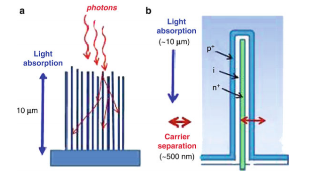
PIN photodetectors made using semiconductor nanowires. Courtesy of Springer
Photoresistors
The mechanism for detecting light in photoresistors is different from the mechanism in photodiodes. Here, the resistance of the material is changed by the incoming light. The change in resistance is sensed by connecting it with a voltage source. The input photons can excite electrons into the conduction band causing increase in the number of mobile electrons which causes the mobility of the material to increase. Photoresistors serve as simple cheap devices to detect light, when not too precise measurements are necessary.
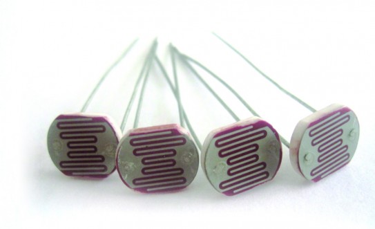
Image of photoresistors with leads for collecting with circuitry. Source FindLight products
Do you use light detection instruments in your devices? What other light detection instruments do you know? Are there any new trends that could take off as the new standard? We would love to hear your comments.
If you are need of light detection equipment, checkout FindLight’s collection of detectors such as avalanche photodiodes, PIN detectors, and photomultiplier tubes. Also checkout CCD devices for more sensitive measurements of light in setups.
