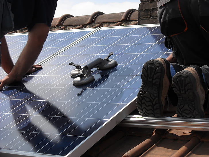
Here we see a solar panel being installed. The role of laser processing is discussed below. Photo courtesy of the U.S. Army.
Introduction
Solar energy is an industry that has gained passionate and widespread support, given its environmental impact. Solar is key to providing sustainable energy and weaning humanity’s dependence on fossil fuels for transportation, industry, energy and more. Adoption is rising across the world, and further research improving panels and their production will gradually increase this adoption.
Unfortunately, high manufacturing costs and the availability of oil weigh down the rate at which the solar industry progresses. Our future most likely hinges on the adoption of solar power before society reaches peak oil. This fact is driving a generation of curious minds to constantly improve solar power and its production processes. New materials, automated tools and machines, manufacturing techniques and packaging are all materializing to streamline and cheapen solar panels for wider distribution.
In the evolution of the solar industry no other manufacturing process has been as vital to the headway of solar cell production as laser-based processes such as cutting, shaping and scribing. In this blog post we will explore the key role lasers play in the solar industry and their important characteristics that make them the ideal choice for EV material processing.

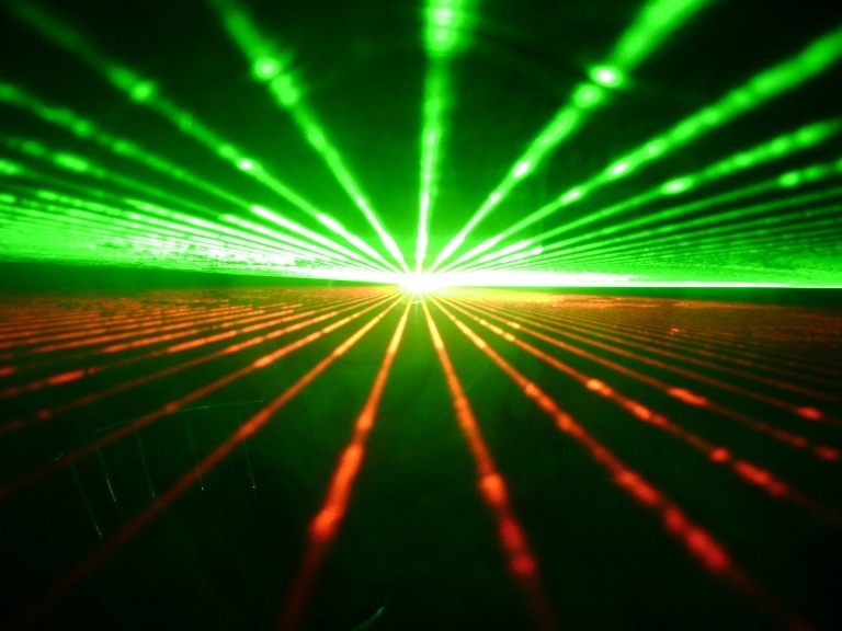
Different laser beams will require unique characteristics to suit each purpose in solar OEM.
What role do lasers play in solar cell manufacturing?
First and foremost a background on the fabrication of solar cells is necessary. Silicon solar cells come in both mono crystalline and thin film fabrications. In monocrystalline cells, silicon wafers composing the cell are sliced from a single crystal with high purity. Thin film cells contain wafers made from amorphous silicon or cast blocks of polycrystalline silicon. In either form, lasers precisely cut and shape the wafers, allowing to put them together as electrovoltaic (EV) cells. In this blog post we will look into the desired beam qualities for solar cell assembly, as opposed to wafer making.
As we mention energy efficiency in this article, it is important to know what composes this measurement. Efficiency can come from reducing the material and labor used during manufacturing. It can also be achieved by maximizing the amount of area solar panels can cover, and the amount of energy they can process. The precision of laser processing has led to more energy efficiency starting at the point of manufacturing. Specifically, laser processing offers higher yields at a lower cost than other deposition methods. It also cuts back on additional materials required for chemical deposition. As we’ll soon see, laser technologies apply to other applications in solar cell manufacturing, with contributing factors that help limit the price per kilowatt produced. Here are four such important use cases:
- Electrical Isolation: a key factor for solar cell efficiency is minimizing energy loss through electrical isolation. This is done by etching the edges of silicon layers. Plasma based edge isolation is the traditional solution, but it uses costly and environmentally harmful etching chemicals. Q-switched lasers with high energy and power can hermetically seal the edges and prevent excess power loss. With laser formed grooves, solar cells experience drastically lower energy losses, down to 2-3% , as opposed to 10-15% that was the standard prior to the adoption of laser technologies.
- Drilling: Besides energy efficiency, laser technologies have made it easier to perform several other tasks in the manufacturing process as well. Drilling wafers with lasers is a common in line practice to conjoin solar modules. Linking solar cells in this way lowers storage costs and improves the overall density each panel achieves.
- Marking: A prominent application of lasers in silicon solar is in marking silicon wafers without inhibiting their conductivity. Wafer marking helps manufacturers track their solar supply chain and ensure consistent quality.
- Ablation: Thin film solar cells rely on vapor deposition and scribing techniques to selectively ablate certain layers for electrical isolation. Thin films need their layers to be deposited quickly without affecting the other layers of glass and silicon. Botched ablation leads to the damage of glass and circuitry on silicon layers, which leads to malfunctioning cells. We explain more on this process in the section below.

Properly soldering and sealing solar cells for maximum efficiency requires a wide variety of measurements. The above formation wouldn’t be possible without laser tech.
What laser power and beam characteristics are ideal?
To ensure stability, quality, and uniformity from panel to panel, laser beam power must be finely tuned for OEM. If laser power cannot meet a certain level, the scribing process will fail. Similarly, the beam must maintain this power within a narrow range and ensure 24/7 “On” time during assembly line manufacturing. All these factors impose very strict requirements on laser specs and necessitate the use of sophisticated monitoring gear to ensure peak operation. For example, laser beam power detectors must have appropriate size and damage threshold to repeatedly test at high powers. Testing power measurements frequently is vital to detect possible failures. In the case of edge isolation, q-switched lasers must have a high-power density to avoid re-deposition of the layers below.
Manufacturers and researchers alike use beam power measurements to customize the laser and tune it to their application. There are many different power measurement tools for wide range of lasers, but in this case, high power detectors can push the limits of lasers under strenuous circumstances. Lasers used in glass cutting, or other deposition applications need a focus on the finer characteristics of the beam as opposed to power.
When ablating onto electronic materials, the characteristics of the beam trump the importance of raw power. Size, shape and intensity play an important role on preventing short circuits in the electronics of the panel. Laser beams ablating deposited PV materials onto the foundational glass panels also need fine-tuned characteristics. As the first point of contact establishing an electrical circuit, the beam must meet all standards. Only a high-quality beam with a fast repetition rate can properly ablate the circuits without damaging the glass beneath. For these purposes, pyroelectric detectors that can measure beam energy even at an extremely high repetition rate are the go-to tool.
The size of the laser beam at its peak influences how and where it will ablate. Beam roundness (or ellipticity) affects the characteristics of scribe lines projected onto the solar panel. Inconsistent beam ellipticity will lead to defective solar panels if scribe lines aren’t uniform. The shape of the overall beam influences the effectiveness of the doping structure on silicon. A variety of lasers result in varying degrees of success. Researchers commonly use Q-switched lasers since their process speeds are limited and not cost efficient. The short pulse required to induce vaporization in solar cells makes mode locked lasers a commonly used choice.
Looking ahead in solar cell manufacturing
New materials like perovskites offer a cheaper and fundamentally different manufacturing processes. Perovskite cell manufacturers use many different fabrication methods for perovskite, the most notable being solution processing, a simple wet chemistry technique. As these processes become scalable and perovskite efficiency meets that of silicon, it may very well become a substitute.
While vapor deposition of perovskite cells uses lasers, the wet chemistry aspect does not. One of the toted benefits of perovskite is that it preserves efficiency while lessening the environmental impact caused by silicon processing and manufacturing. As researchers make headway in their exploration of these new materials, laser processing might eventually take a back seat.
The amount of progress that is taking place in laser processing technology is astounding. Much of this speed is attributable to the research that has gone into improving solar cells. With the variety of beam diagnostic options, both novices and experts can properly measure their light sources in compact, portable settings in just about any environment. For these reasons, lasers are the most reliable way to produce silicon solar cells. It will no doubt be a staple for the near future.
This article has been sponsored by Gentec-EO, who supply beam measurement tools that can be used in many of the applications listed above, as well as other laboratory, OEM and research needs.
