Organic Light-Emitting Diodes (OLEDs) are most famously known for their use in foldable smart phone displays. From the Samsung Galaxy Fold to the Huawei Mate X (2019), these devices offer huge screens that can fold down to the size of a more traditional smartphone screen. This revolutionary new technology is made possible by the properties and composition of OLED screens. In traditional Liquid Crystal Display (LCD) screens, a glass pane covers the actual liquid crystal display that emits the light. On the other hand, OLED screens have the light emitting technology already built into them. Thus, when you touch interact with an OLED device, you are touching the actual display too. OLED screens are often made of a type of plastic, which allows for flexibility and folding screens. These devices also require OLED color patterning techniques in order to integrate color into the display devices, which we will describe further in the upcoming sections.
Intro to OLED Composition
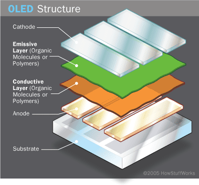
Now, we will brief on the composition and integration of OLED technology in this plastic screen. OLEDs are made of two or three organic layers sandwiched between two electrodes (cathode and anode) on top of a substrate layer. The organic layers and electrodes emit light in response to an electric current. One of the most difficult processes in manufacturing these OLEDs is attaching the organic layers to the substrate. For example, organic vapor phase deposition and inkjet printing are both efficient methods that can reduce the cost of producing OLED displays.

OLED components include organic layers that are made of organic molecules or polymers. This diagram is a two (organic) layer model.
Courtesy of HowStuffWorks.
Another big part of OLED manufacturing is the color patterning step, which allows the OLED device to display color. There are various methods in use for OLED color patterning, including photolithography. Lithography is commonly used for semiconductors and TFTs, but presents challenges for OLEDs. This is due to the high temperature and humid conditions required for attaching OLED layers together. In this article we will explore three different color patterning technologies that have arisen for more efficient and accurate OLED optical manufacturing.
OLED Color Patterning and Masking Techniques
Error produced in processing an OLED with a red pixel mask. We can see that the spacing in the pattern is off around the red arrow. Courtesy of Tsujimura.
The resulting color variation in OLED screen due to shadow mask deformation. shown above. Courtesy of Tsujimura.
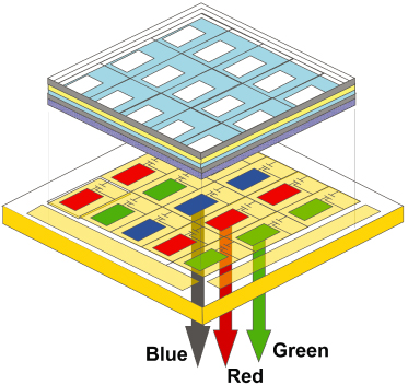
Second, we have the “Color Filter Method” a.k.a. “White+Color Filter Patterning” method. In this method, the OLED itself is also designed and manufactured with all three color elements in each pixel. However, different from the “Shadow Mask Patterning” method, these OLEDs only produce white light. Next, additional red, green, and blue color filters are utilized to match the desired color output. Accordingly, this process allows for a dynamic range of colors to be emitted with different levels of filtering. However, a big consequence of using color filters is that the purity of the image may be compromised due to interactions of the OLED light and physical color filters. Equally important is the high power consumption this method eats up. Because the color filters absorb most of the light intensity, the process requires a constant, powerful back light.

Schematic diagram of White+Color filter patterning method for OLEDs. Courtesy of Tsujimura.
Rising OLED Color Patterning Techniques: Electron Beams
In 2016, a new approach for OLED color patterning was developed at the Fraunhofer Institute for Organic Electronics. Researchers utilized electron beam technology to color pattern the organic layers in the OLED. Because this process acted on the micro-scale, it produced extremely accurate, high-resolution results, even with the help of color filters. Further, it also allowed for complex patterns and high-definition (HD) grayscale images. Since then, this technology has been developed and advanced to that of full-color working OLED displays, without the use of external filters.
Now, we will discuss an overview about how the electron beam process works. First, an OLED is produced containing all three RGB organic emitting layers. Akin to the previously mentioned processes, this OLED is designed to produce only white light. Next, a thermal electron beam is directed on the white emitting OLED. The electron beam excites certain molecules in the organic layer of the OLED, which causes the molecules or atoms to separate and become structured. Consequently, the thickness of different areas in the OLED organic layer changes and pixels with distinct colors (RGB) are formed. Moreover, the electron beam patterning process allows for microstructuring into color pixels without perturbing the other substrate and electrode layers.

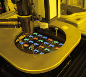
Probe station with patterned OLEDs in the clean room.
Courtesy of Fraunhofer FEP.
Conclusion
As more AMOLED, and flexible displays enter the market, OLED technology will continue to become more popular and widespread. One of the most important considerations for OLED availability in mass market, is in screen color production. Rising techniques such as the Electron Beam Patterning method can produce high quality, low cost, and energy efficiency. Another key consideration in OLED screen production is low material consumption. Further rising techniques in research that allow for low material costs include the vapor injection source technology (VIST) method, hot‐wall method, and organic vapor‐phase deposition (OVPD) [1].
This article is made possible by Gentec-EO, the market leader in the manufacture of light detection devices.
Further Reading
[1] https://onlinelibrary.wiley.com/doi/10.1002/9781119187493.ch5
