Introduction
As electronic devices continue to become faster and more complex, designing high-speed printed circuit boards (PCBs) with excellent signal integrity becomes critical. High-speed PCB design involves a range of challenges, from managing signal reflections and crosstalk to controlling impedance and ensuring proper grounding. In this article, we’ll provide a comprehensive overview of tips and techniques for designing high-speed PCBs with excellent signal integrity. Whether you’re designing a simple board for a personal project or a complex system for a commercial application, these tips will help you optimize your design for maximum performance and reliability.
Understanding the Fundamentals of Signal Integrity: Signal Reflections, Crosstalk, and Timing Analysis
High-Speed PCBs
Signal integrity is a critical consideration in high-speed PCB design. When signals travel along a trace, they can encounter reflections that bounce back and forth, causing noise and timing issues. Crosstalk can also occur when two or more signals interfere with each other, leading to signal degradation or loss. To minimize these issues, designers need to have a solid understanding of the fundamentals of signal integrity. By analyzing the characteristics of the signals and the transmission lines, designers can use tools like time-domain reflectometry (TDR) and frequency-domain analysis to identify potential signal integrity problems and optimize their designs for maximum performance.
Time Domain Reflectometry (TDR)

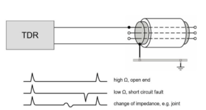
TDR-measurement, typical setup. Photo courtesy of HV Technologies
Time-domain reflectometry (TDR) is a technique that has been widely used in the field of high-speed PCB design to measure and analyze the impedance and signal integrity of transmission lines. A transmission line is a structure that carries electrical signals from one point to another, and it consists of conductive traces, vias, and other components. A transmission line with proper impedance matching, well-managed parasitics, and a low level of crosstalk can ensure the high quality and reliability of the signal.
TDR works by injecting a fast electrical pulse into the transmission line and then measuring the reflections that occur when the pulse encounters any impedance mismatches or other signal disruptions. The reflected signals are analyzed in the time domain to determine the transmission line’s properties, such as characteristic impedance, propagation delay, signal attenuation, and other parameters. TDR is a valuable tool for troubleshooting signal integrity issues and verifying the performance of high-speed PCB designs, making it an essential technique for modern electronics design.
High-Speed PCB Design Techniques: Trace Routing, Via Placement, and Grounding Strategies
High-speed PCB design requires careful consideration of trace routing, via placement, and grounding strategies. Routing traces correctly can help minimize reflections and crosstalk, while via placement can impact impedance and signal integrity. Grounding is also a critical consideration since it provides a low-impedance path for return currents and helps reduce noise. To optimize their designs, designers need to carefully plan the placement and routing of traces and vias, considering factors such as trace length, spacing, and width, as well as via size and placement. They should also carefully consider the grounding scheme, including the use of ground planes, stitching vias, and split planes.
Trace Routing
Trace routing is a critical aspect of PCB design, particularly for high-speed circuits. When designing PCBs, trace routing techniques are employed to ensure signal integrity and prevent issues such as crosstalk and signal distortion. To optimize trace routing, designers can use several techniques, including:
- Differential Pair Routing: This technique is used for high-speed differential signals that involve two conductors with equal but opposite signals. Differential pairs are commonly used in circuits such as USB, Ethernet, and HDMI, and they require careful routing to ensure signal integrity. This technique involves routing two traces with equal and opposite signals next to each other, with a ground plane or signal reference plane between them to reduce crosstalk and interference.
- Matched Length Routing: This technique ensures that all traces in a group have the same electrical length. This is important for signals that need to arrive at the same time, like data and clock signals. By keeping the length of each trace the same, the signals can arrive simultaneously, reducing the risk of timing errors.
- Length Tuning: This technique is used to ensure that signals arrive at their destination at the same time. Length tuning involves adjusting the lengths of the traces in a group to ensure that they all arrive at the same time, reducing timing errors and improving signal quality.
Via Placement Techniques
Via placement is another critical aspect of high-speed PCB design. Vias are used to connect the different layers of the PCB and can impact signal integrity and impedance. Some common via placement techniques include:
- Via-in-Pad: This technique involves placing a via in the pad of a surface mount component. This technique can help reduce the inductance of the via and improve signal integrity.
- Blind Vias: These vias only connect the top layer of the PCB to one or more inner layers, allowing for more routing space on the outer layers of the PCB. Blind vias can help reduce signal reflection and improve impedance.
- Buried Vias: These vias connect the inner layers of the PCB and are not visible from the outer layers. Buried vias can help reduce signal reflection and crosstalk.
Grounding Strategies
Grounding is a critical consideration in high-speed PCB design. Proper grounding provides a low-impedance path for return currents and helps reduce noise. Some common grounding strategies include:
- Split Planes: This technique involves dividing the ground plane into smaller sections, with each section connected to a separate ground pin on the PCB. Split planes can help reduce noise and improve signal integrity.
- Stitching Vias: These vias connect different ground planes or sections of a ground plane, reducing the impedance of the ground connection and improving signal integrity.
- Via Fences: These are rows of vias placed around the edges of the signal traces to reduce electromagnetic interference. Via fences can help reduce crosstalk and signal distortion.
Managing Impedance in High-Speed PCBs: Calculating Impedance and Using Controlled Impedance Routing
Strip-layer configurations. Photo courtesy of PCB Cadence
Impedance is a crucial factor in high-speed PCB design, as it affects signal quality and reliability. To manage impedance, designers can use controlled impedance routing techniques, which involve adjusting the width and spacing of traces to achieve a specific impedance value.
Impedance calculation methods include formulas, online calculators, and simulation tools. Formulas are based on the physical characteristics of the transmission line, such as the trace geometry, dielectric constant, and copper thickness. Online calculators and simulation tools can help designers optimize their designs and ensure that the signal quality meets the required specifications.
Impedance matching techniques, such as series resistors, parallel capacitors, and tapered traces, can be used to adjust the impedance of a trace to match the source and load impedances.
Controlled impedance routing techniques include micro-strip, strip-line, and dual strip-line. Micro-strip routing involves placing the signal trace on top of a ground plane, while strip-line routing involves placing the signal trace between two ground planes. Dual strip-line routing is similar to strip-line routing, but with an additional ground plane on the opposite side of the board.
Designing and Testing High-Speed PCBs: Best Practices and Validation Techniques

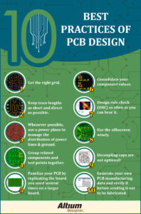
PCB Design practices. Photo courtesy of Altium
Designing and testing high-speed PCBs requires careful planning and execution. Before finalizing the design, designers should perform simulations and analyses to identify potential issues and optimize their designs.
Signal integrity analysis techniques are used to verify that signals are propagating through the circuit as intended, without being degraded or distorted. Eye diagram analysis is a common technique that involves plotting the received signal over time and voltage, and examining the shape of the resulting “eye” to determine the quality of the signal. Jitter analysis is another important technique that measures the variation in timing of digital signals, which can be caused by a variety of factors such as noise, crosstalk, and power supply fluctuations. Time-domain reflectometry (TDR) is also commonly used to measure the impedance and reflection characteristics of transmission lines.
Power integrity analysis techniques are used to ensure that the power distribution network is stable and can provide adequate power to all components on the board. Power plane analysis involves measuring the voltage drop and current density across the power planes to identify any areas of excessive current or voltage drop. Decoupling capacitor placement is another important consideration for power integrity, as it helps reduce noise and stabilize the power supply.
EMI/EMC testing techniques are used to ensure that the board complies with electromagnetic interference (EMI) and electromagnetic compatibility (EMC) regulations, which are necessary for the device to function properly and not interfere with other electronic devices. Radiated emissions testing measures the electromagnetic field emitted by the board and ensures that it is within acceptable limits. Conducted emissions testing measures the amount of electrical noise that is conducted through the power and ground connections of the board.
Conclusion
In conclusion, high-speed PCB design is essential for electronic devices to operate efficiently and reliably. To achieve optimal signal integrity, designers must consider many factors, including signal reflections, crosstalk, and timing analysis. By understanding the fundamentals of signal integrity and utilizing techniques such as TDR analysis, designers can troubleshoot issues and optimize their designs for maximum performance. Trace routing, via placement, and grounding strategies are critical considerations for high-speed PCB design. Techniques such as differential pair routing, matched length routing, via-in-pad, blind vias, and split planes can significantly improve signal integrity and reduce noise. Properly designed high-speed PCBs can ultimately result in the efficient operation and long-term reliability of electronic devices.
External Sources
If you’d like to read more on high-speed PCB conventions:
https://www.hvtechnologies.com/the-basics-of-time-domain-reflectometry-tdr/
https://resources.pcb.cadence.com/blog/2021-signal-integrity-fundamentals-in-pcb-layout
https://resources.altium.com/p/what-high-speed-design
https://www.protoexpress.com/blog/best-high-speed-pcb-routing-practices/
https://resources.altium.com/p/10-best-practices-of-pcb-design
