Edge emitting and surface emitting lasers present two configurations for laser emission using semiconductors. Edge emitting lasers came first but were quickly replaced by surface emitting lasers for telecommunication applications. However, single edge emitting lasers can offer higher power than surface emitting lasers. Various factors in the design process of these devices affect the overall stability, reliability, and yield of these devices. This article will detail the fabrication process and uses it to compare and contrast the performance and yield characteristics of these two types.
Fabrication
Fabrication of edge and surface emitting diode lasers has been possible with better fabrication methods such as molecular beam epitaxy (MBE). The semiconductor wafer is patterned and precisely controlled in thickness as overlayers are deposited vertically to develop the structure. The image below shows the growth and processing methods for VCSELs, which are a type of surface emitting laser, as well as for edge emitting lasers.
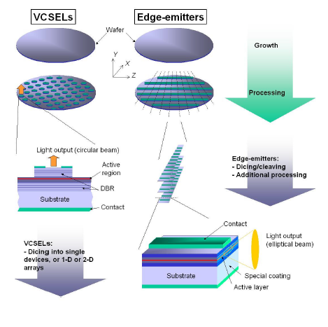
Growth and processing of surface and edge emitting lasers. Courtesy of Princeton Optronics
After patterning and MBE deposition of the semiconductor layers, the top contact is deposited for both structures. The next step is the dicing of the wafer. For surface emitting lasers, this process does not involve cutting edge facets in the laser. In contrast, for edge emitting diodes, the lasers are fully created only after dicing the wafer. Because of this fundamental difference, edge emitting lasers cannot be tested as they are grown. The dicing process is crucial for edge emitting lasers and irregularities can reduce yield and reliability.
Edge Emitting Lasers
In an edge emitter, the light bounces back and forth horizontally as shown in the below image. The optical cavity is a Fabry-Perot cavity with the end facets acting as reflectors. The difference in the index of refraction between the air and the gain medium causes reflection at the end facets. Since the end facets are created by cleaving, a high degree of smoothness is hard to obtain. Moreover, edge emitting lasers also suffer form catastrophic optical damage (COD) at the facets, a common problem reducing reliability in laser diodes. VCSELs do not show this damage as the end facets are designed differently.
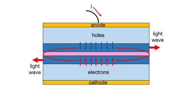
Light bouncing back and forth in an edge emitting laser before being emitted out.
Because of the geometry of the design, the vertical thickness of the active region is small compared to the horizontal width. Thus the laser output will not be a perfect circular Gaussian beam, but instead squeezed in one direction. Additional optical lenses are required to make the beam Gaussian and for efficient coupling into optical fibers. Because the active medium is surrounded by lower refractive index materials, the laser light is naturally guided providing no need for additional confinement techniques.
There are some advantages that can be noted compared to VCSELs. Edge emitters can host multiple modes while lasing compared to single mode emission in surface emitting lasers. Moreover, the gain length is higher in edge emitters and can give higher output powers from a single diode in some designs. Initially edge emitters were used for fiber optic communications, but quickly fell out in favor of surface emitting lasers such as VCSELs which offer more precisely controllable wavelengths.
Surface Emitting Lasers
Apart from the perceived small decrease in total gain in comparison to edge emitters, surface emitting lasers offer a lot of advantages in terms of yield, stability, cost, and testing. VCSELs in tens of GHz have been manufactured for fiber optic communications.
The main gain medium is a series of quantum wells with the top and bottom layer being reflectors. Normal mirrors cannot be used to reflect light so instead Bragg reflectors are used for a compact setup. Some designs let the other side of the cavity to be free of reflector for surface emitting external cavity lasers. A Bragg reflector can be made with alternating layers of GaAs and AlAs with the thickness chosen to be quarter of the wavelength of the gain bandwidth center frequency.
The whole setup can be tested as it being fabricated in millions on the same wafer and thus there is better process control in case the parameters are a little off during growth. This helps increase the yield of surface emitting lasers by ten fold compared to edge emitting lasers. The output light bounces up and down instead of left and right. Since there is no natural way to guide the light in VCSELs such as index waveguiding in edge emitters, additional layers for photon confinement are added at the top sometimes. Also layers for current confinement are added to control the spread of injected electrons and holes for increased recombination efficiency in the active region. The image below shows a cross-section of a VCSEL device.
Layers in a surface emitting laser such as VCSEL. Courtesy of Photonics.com
Table of Comparison
The spectral linewidth of surface emitting lasers, such as VCSELs, can be made very narrow (<5 nm) compared to emission from edge emitting lasers and LEDs. The wavelength does vary with temperature as shown below.
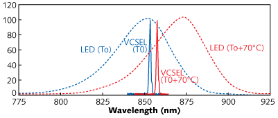
VCSELs show smaller drifts in wavelengths with temperature. Courtesy of myVCSEL
Because of the vertical growth geometry in VCSELs, they can be diced and packaged easily, and as yield is high, the average cost is low compared to edge emitting lasers. VCSELs are more reliable as they do not undergo catastrophic optical damage. The table below compares the various properties of VCSELS and edge emitting lasers.
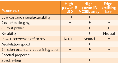
Comparison of properties between VCSELs and edge emitting lasers. VCSELs offer many advantages. Courtesy myVCSEL
High Power Laser Applications
Solid state and gas lasers are used for high power applications with involve cutting, drilling, and micromachining. The need for higher power density in laser beams increases each year, almost linearly like in Moore’s law. Thus trying to get diode lasers into the high power regime can provide more compact, lower cost designs.
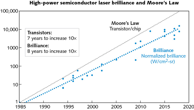
High power semiconductor lasers vs year. Courtesy of Laser Focus World
Diode lasers are not usually the first choice for high power applications, but new designs with laser arrays can help laser diodes enter the high power market.
Interested in compact laser applications for your projects? Check out FindLight’s collection of surface emitting VCSELs, CW diode lasers, swept laser systems and fiber coupled diode lasers.
