The electron can provide lots of information about a material’s surface in electron spectroscopy studies. Traditionally, electron spectroscopy uses the characteristics of electrons emitted from materials to study material properties. When a photon or an electron hits a surface, the characteristic electrons can act as messengers by exhibiting characteristic energy levels, revealing lots of chemical information about the elements and their electronic structures. Auger or photoelectrons can only escape from the uppermost atomic layers of solid (a depth of 10 nm or less) because their energies are relatively low (generally 20–2000eV), while the characteristic X-rays can escape from a much greater depth (several micrometers from the surface).
X-Ray Photoelectron Spectroscopy (XPS)
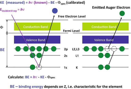
XPS is a variety of electron spectroscopy. The X-ray photoelectron is an electron ejected from the electron shell of an atom when the atom absorbs an X-ray photon. An incident X-ray photon has enough energy (hv) to knock out an electron located in the inner shell, such as the K shell. With kinetic energy, we can calculate binding energy which leads to characteristic values of atomic electrons. From that we can identify what elements are present.
Auger Electron Spectroscopy (AES)
Auger electrons were named after Pierre Auger who, together with Lise Meitner, discovered Auger electron emission in the 1920s. When a high energy electron or X-ray photon knocks out an electron located in the inner shell, the atom becomes ionized and goes into an excited state. An electron located in the outer shell would refill the vacancy in the inner shell so that the atom can return to the normal state. However the emission of either an Auger electron from an electron outer shell or a characteristic X-ray photon would occur because of the energy difference between the outer-shell electron and the inner shell. The kinetic energy of an Auger electron is approximately equal to the energy difference between the binding energies in the electron shells involved in the Auger process. The signals from Auger electrons are relatively weak compared with those of secondary electrons that have escaped from a solid surface.
Electron Spectroscopy Instrumentation
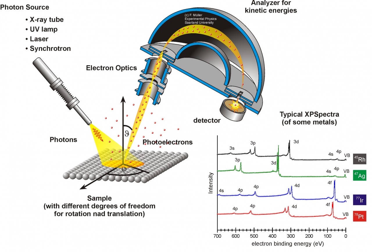
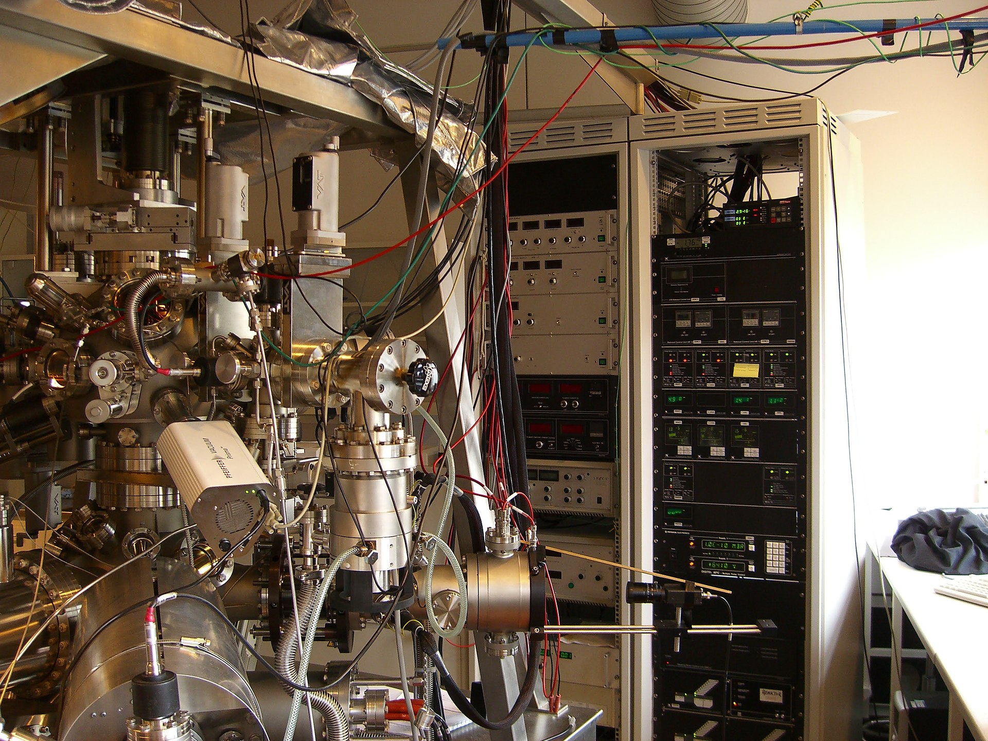
Structure of an electron spectrometer. Courtesy of AG Jacobs.
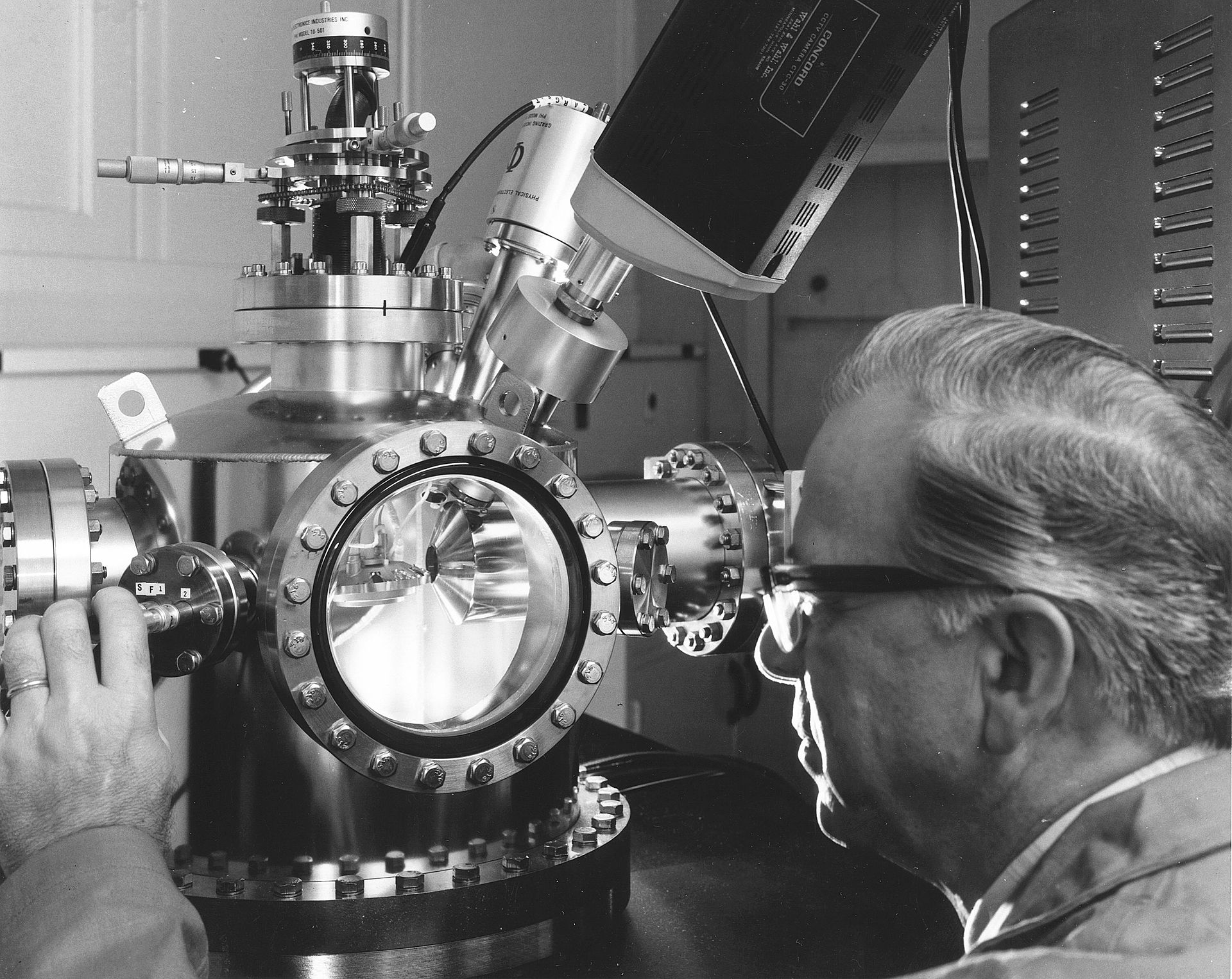
A multifunctional surface analysis system for electron spectrometry contains XPS, AES and a scanning electron microscope (SEM). So this system includes an electron gun, an X-ray gun, and a shared analyzer of electron energy. These instruments also require a ultrahigh vacuum environment so that the chances of low- energy electrons being scattered by gas molecules on their way to reach the detector can be reduced and the sample surface would not be contaminated by gas molecules.
Source Guns for Electron Spectroscopy
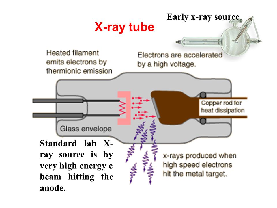
X-ray photons are generated by high-energy electrons striking a metal anode, commonly Al or Mg for XPS spectrometry. The X-ray gun produces a characteristic X-ray line to excite atoms of the surface to be analyzed. For AES analysis we use the electron guns to shoot electron beams with kinetic energy. We also use ion guns for electron spectrometers. It can clean the sample surface which is commonly contaminated with adsorbed hydrocarbons, water vapor, and oxides before examination. In addition, it can reveal the depth profile of an element by sputtering out sample atoms layer by layer.
Electron Energy Analyzer
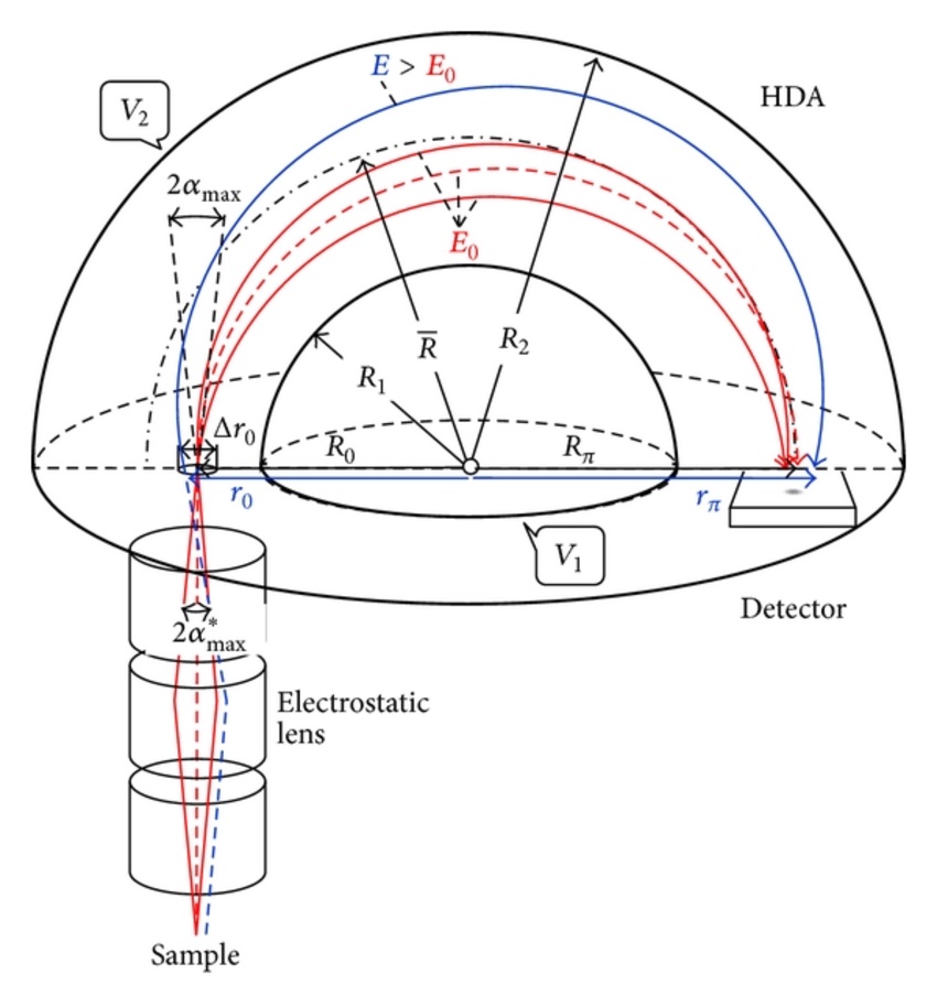
We can use an electron energy analyzer to obtain XPS and Auger spectra for electron spectrometers. The most commonly used analyzer is the concentric hemispherical analyzer (CHA). The analyzer is composed of two concentric hemispheres with radii R1 and R2. Negative potentials V1 and V2 are applied to the inner and outer hemispheres, respectively. So we have a median equipotential (Vo) surface in the middle with radius of R. Before entering the CHA, electrons are focused by an electrostatic transfer lens to lower the energy level. Then the electrons enter from a slit from one end of CHA from the sample. Then the CHA only allows the electrons with energy Eo =eVo to pass through and reach the detector.
Characteristics of Electron Spectra
XPS spectra are expressed as photoelectron intensity versus binding energy (EB). There are three types of peaks on an XPS spectrum background. The photoemission from core electron level peaks are the primary peaks for element analysis. The photoemission from valence levels peaks with low binding energy are useful for the analysis of material’s electronic structure. The Auger emission excited by X-rays peaks are for chemical analysis. Each peak represents the amount of electrons at a certain energy that is characteristic of some element.
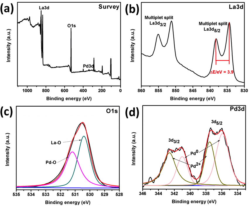
Examples of XPS spectrum of Pd/La(OH) 3 nanocatalyst (a), High resolution XPS spectra of La3d (b), O1s (c) and Pd3d (d) orbitals. Courtesy of researchgate.net.
Auger spectra are expressed in direct and differential modes. The direct mode presents the intensity distribution and the differential mode presents the derivative of intensity versus the kinetic energy. We often examine the derivation to better see distinct features.
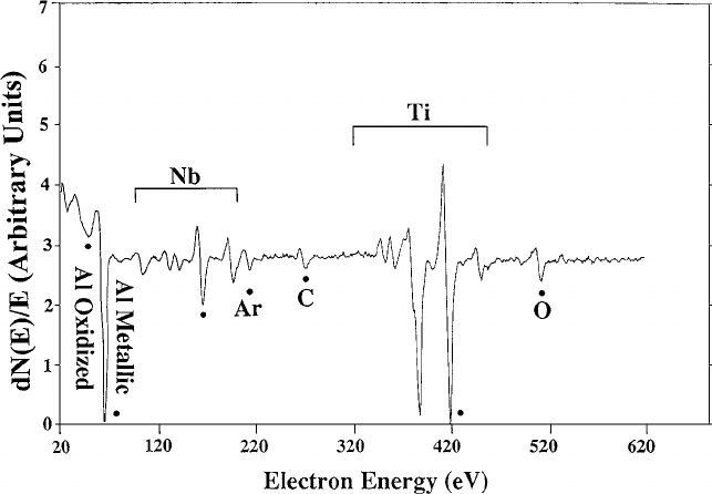
Example of the Auger spectrum of Ti-44Al-11Nb sample after 105 minutes Ar ion sputtering. Courtesy of researchgate.net.
Qualitative Analysis
XPS and AES are powerful tools for surface chemical analysis. They can identify chemical elements in the layer within several nanometers from the surface. If Binding Energy (BE) is displayed, XPS peaks are independent of incident x-ray energy while AES peaks shift with x-ray energy.
Peak identification in AES spectra is straightforward. After the spectrum is plotted you can look for the designated value of the peak energy from the graph and find the element present on the surface. Peak identifications in XPS spectra are more complicated because of the Auger peaks. So we need to use two different X-ray sources to distinguish the Auger peaks from photoelectron peaks.
Chemical shifts of binding-energy peaks for an element are caused by the surrounding chemical state of the element. When an atom bonds to a more electronegative atom, it becomes slightly positive and the BE of its remaining electrons increases. So we often fit detailed spectra to determine the chemical environment of individual elements which is critical to identify the peaks correctly.
XPS Application in Industry
XPS can provide information about surface layers or thin film structures including polymer surface, catalysts, corrosion, adhesion, semiconductors, dielectric materials, electronics packaging, magnetic media, thin film coatings.
For example, utilizing the XPS to get battery material information on the chemical reactivity and associated stability of electrochemical interfaces over a wide spatial range varying from microscale to mesoscale information such as chemical states and distribution.
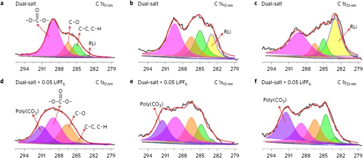
XPS spectra of C 1 s (a–c) from Li-NMC batteries with dual-salt electrolyte and XPS spectra of C 1 s (d-f) from Li-NMC batteries with 0.05 M LIFP6 added dual-salt electrolyte after 2 formation cycles and 10 charge/discharge cycles. C0nm, C10nm , and C25nm , indicate the depths at the XPS measurements were performed. Courtesy of ScienceDirect.com.

What’s the reason we get satellite peaks in a XPS ???