New graphene-silicon blended devices can bring about great advancements in a number of areas, with thermal energy storage being among them. Image courtesy of wikipedia.org.
Improving Communications by Blending Materials
The advances in communication technologies that we enjoy today and treat as granted in our everyday lives are a result of a formidable thrust in the advancement of photonics – a research area that studies light. Today, people use more handheld electronic devices than they did in the past; smartphones, tablets and wearables are only examples. At the University of Delaware, Professor Tingyi Gu, is one of the many people working on cutting edge photonics research. His work and those of his students involves developing devices that will enable faster communication between pieces of technology. Recently, they developed a revolutionary graphene-silicon device in order to speed up communications between pieces of technology. In particularly, they discovered a way of placing the graphene in a special place known as the p-i-n unction, or the interface between different materials. This approach drastically improved the responsiveness and the speed of the devices.

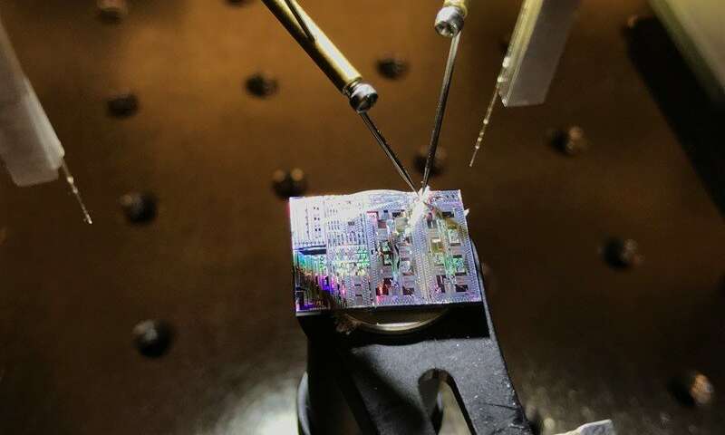
An example of what a graphene-silicon device might look like, illustrating the work at the University of Delaware Nanofabrication Facility. Image Courtesy of the University of Delaware and phys.org.
Limitations of Silicon and Advantage of Graphene
Many people these days are familiar with the incredible benefits of silicon in technology. Different silicon photonics devices provide benefits in many areas including multi-channel mode (de) multiplexers and polarization beam splitters.
While silicon is naturally occurring, exists widely, and is commonly used as a semiconductor, it comes with problems. Semiconductors made exclusively of silicon have limited carrier mobility and an indirect bandage. As a result, light moves through the material more slowly and these devices have a limited ability to release and absorb light.
Gu’s team combined silicon with 2-D graphene to overcome some of these issues. Graphene is known as a 2-D material because it is composed of just a single layer of atoms. The engineers use graphene because graphene has better carrier mobility and direct bandage. Graphene can also transmit electrons more quickly, along with having better electrical and optical properties. As discussed by Daniel Neumaier from AMO GmbH, Leader of the Graphene Flagships Division on Electronics and Photonics Integration, graphene-silicon devices may even be the most promising possibility for increasing the speed and reducing the power and footprint of key components of silicon photonics technology with a single chip.
Breaking Down the Specific Benefits of Graphene
Graphene has tunable optical properties, high electrical mobility, and spectrally broadband operation compatibility with silicon photonics. Additionally, it absorbs uniformly across a broad range in the visible and infrared spectrum. This allows for the monolithic integration of phase and absorption modulators, switches, and photodetectors.
Furthermore, since many devices already use silicon devices, it can be adopted more quickly than other potential solutions. This is because scientists may be able to continue to utilize technologies that already contain silicon devices by simply adding a graphene component to those devices. Consequently, it would be a simple adoption of a new area of research by adding to something that already exists rather than a massive overhaul that would require multiple replacements.

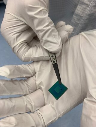
The team at the University of Delaware engineered a graphene-silicon device. This device can transmit radio frequency waves in less than a picosecond at a sub-terahertz bandwidth. Image courtesy of the University of Delaware and phys.org.
Understanding How Technology is Implemented and Potential Applications
There are many key factors to consider with these graphene-silicon devices. As mentioned previously, Gu and his team made these devices by placing the graphene in a special place known as the p-i-n junction, or the interface between the materials. This approach is beneficial because it is robust and easy to apply.
These devices might enable rapid advancements in such wide fields as optoelectronics, biomedicine, and plant science. However, perhaps the most widely known imminent application for these graphene-silicon devices is with photodetectors. These types of detectors sense light and produce current. These graphene-silicon devices might lead to technologies with more bandwidth and a lower response time. In other words, the technologies will potentially produce more power and will transmit energy signals more quickly.
Earlier Work with Graphene
Other groups besides Gu’s have seen the advantages of combining graphene with silicon in different devices for next-generation data communications. One example of this occurred with researchers from the Graphene Flagship initiative. This initiative worked with the world’s first high-speed graphene-based data communication at a data rate of 50 Gb/s. The initiative includes such well renowned flagship partners as AMO GmbH from Germany, and the Institute of Photonics Sciences (ICFO) from Spain. The research findings from this initiative and others formed the early motivation for the work on these graphene-silicon devices.
Thermal and Energy Applications
Among many potential applications for graphene-silicon devices, their possible use for energy related applications is noteworthy. Using these devices for thermal-tuning/switching might improve the limitations that exist in traditional constructs. New graphene-silicon devices can utilize the thermal-optic effect since there is no special requirement for the waveguide materials. Often times, scientists use metal heaters in this area of research that have maximum temperature heating limits. However, since graphene has very high thermal conductivity (up to 5300 W/(m*K)) at room temperature and a high optical damage threshold, it might be possible to eliminate this issue with these devices. Therefore, thermal conduction for gathering and storing energy can occur more quickly, the devices can have improved responsiveness, and an improved range of operating temperatures.
It is rather evident that there are many applications for blending graphene and silicon together and few downsides. Ultimately, scientists and engineers will need to conduct more research to determine how to best use this new technology in various applications.
