Motivation behind advancing micro welding technologies
One of the important technologies for attaining complex goals and providing high quality requirements for the electrical and mechanical connection in the manufacturing of electro mobility components is laser material processing. For cutting materials, creating battery cell housings, and joining conductor materials to battery cells, laser beam sources are employed. In this article, we specifically discuss the technology of laser micro welding with applications to copper. This article is mainly based on the research conducted by scientists at WTH Aachen University.
Connector materials for common applications range in thickness from 100 to 300 micrometer for cylindrical battery cells and between 250 and 300 micrometer for the battery housing. The development of fiber laser beam sources with a wavelength in the near infrared range (1030–1070 nm) is the main objective for welding these materials with quick processing times and little energy input.
Under 5% of the laser energy is absorbed by the copper materials used for electrical contacts in this wavelength range. The method can now take advantage of absorptivity of up to 50–60% at ambient circumstances by creating laser beam sources in the blue wavelength range (450 nm).
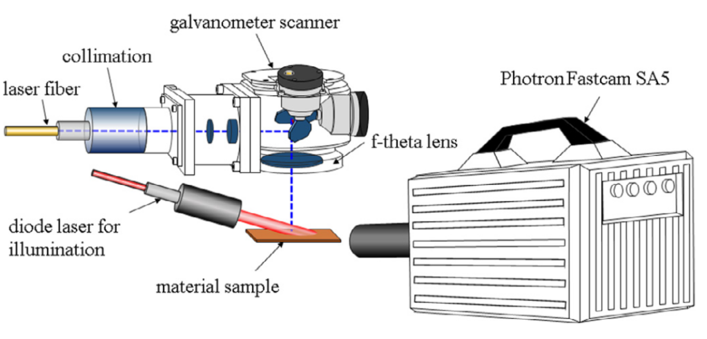
Figure 1: Optical setup including high-speed videography. Image courtesy of Elsevier
This situation makes it possible to create processes that are more accurate and manageable than before. The use and development of blue laser beam sources are currently being studied. It was first reported in 2017 that a laser beam source with a wavelength of 450 nm and enough laser power for laser beam micro welding had been created.
Blue laser beam and micro laser welding
The AO-150, the first commercially available diode laser with a wavelength of 450 nm and an output power of 150 W, was subsequently created by Nuburu Inc. Using a blue laser beam source (see Figure 1), preliminary research on copper foils with a thickness of 125 m demonstrates that copper may be welded without splashes or pores.
Pore development in heat conduction welding is also preventable. The primary focus of development is already on laser beam sources with enhanced beam quality and greater laser powers of up to 1.5 kW. For bead-on-plate welds, laser systems still in development with output powers more than 500 W can weld to depths greater than 300 m at a feed rate of 4 m/min.
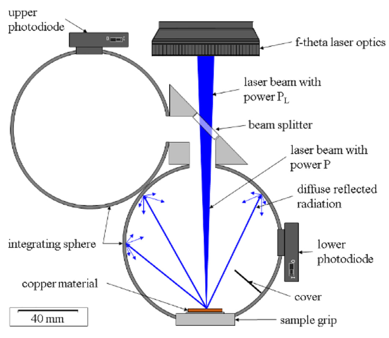
Figure 2: Experimental setup of the integrating spheres. Image courtesy of Elsevier
Experimental setup of laser micro welding
The utilization of fixed optics with a high-speed axis (see Figure 1 and Figure 2) moving the material sample through the laser beam is a common feature of all conducted experiments. The laser system AO-150 from Nuburu Inc. is employed in this study’s experiments and has a wavelength of 450 nm.
The laser is implemented within an optical configuration based on a scanner. Cu-ETP and CuSn6 welding is carried out using a thorough examination of the laser absorption that occurs throughout the procedure. In order to study the process on the material surface, high-speed videography (see Figure 1) is employed to separate the process into distinct phases. The constraints of a scanner application with the employed laser beam source are explored using technically significant joint configurations as butt and overlap joints.
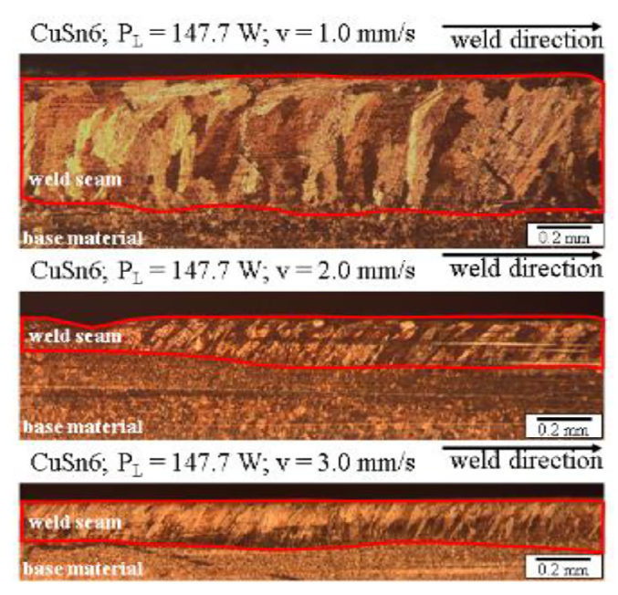
Figure 3: Longitudinal sections of CuSn6. Image courtesy of Elsevier
Results and discussion
Drude model
A heat conduction model is used to complement the investigations in order to categorize the laser beam sources and provide a roadmap for potential 450 nm uses in the future. Numerous internal processes of the material must be taken into account in order to theoretically explain the absorption of electromagnetic waves on the surface of metallic materials (for example see Figure 3).
However, the precise calculation of the absorption is only possible to a limited extent because factors like the geometric properties and the chemical composition of the surface have to be known with accuracy. In practice, a qualitative description of the electric properties can already be obtained from the straightforward Drude model.
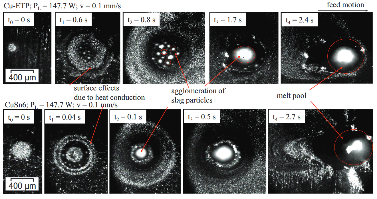
Figure 4: High speed videography of laser welding processes of Cu-ETP and CuSn6. Image courtesy of Elsevier
Absorptivity
An experimental approach is required to ascertain the wavelength dependent absorptivity of various materials. The absorptivity rises with decreasing wavelength for all metallic materials that have been examined. Cu-ETP exhibits an increase in absorptivity from 2.5% at 1070 nm to 68% at 515 nm (see Figure 4). For CuSn6, the same behavior is seen. Here, the absorptivity rises to 70% from 9.5%.
Aluminum also shows an increase, but it is less pronounced than it is for copper-based products. At a wavelength of 808 nm, the maximum absorptivity is around 24% in this case. The absorption coefficient does not rise further since the wavelength keeps getting shorter. A sizable rise can be seen for aluminum alloys like AlMgSi1 (see Figure 5).
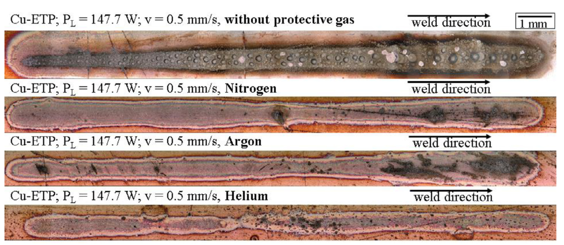
Figure 5: Influence of protective gases on welding results. Image courtesy of Elsevier
Effect of material properties and protective gases
The employment of laser beam sources with a wavelength in the range of 450 nm results in a higher absorptivity during the welding process, particularly in welding applications between copper and copper alloys. A Nuburu AO-150 diode laser beam source with a wavelength of 450 nm is employed for the experimental setup. Two distinct laser power levels will be applied in this investigation. After the focusing lens, 147.7 W of output power is available.
A laser power of 131.7 W is available on the material surface inside the experimental setup of the integrating spheres (89.14% transmittance of the beam splitter). This maximum laser power will be used for the experiments that follow. Heat conduction welding is carried out using a scanner-based method because of the qualities of the laser.
A Photron Fastcam SA5 is also used to view the welding process. High-speed videography makes it possible to observe process dynamics in great detail. A diode laser emitting at 808 nm is included in the setup to provide process illumination. On the high-speed camera, an optical broadband filter for 808 nm is utilized. The preparation of cross sections allows for additional observation of the samples of welded material.
On specimens of Cu-ETP and CuSn6 with dimensions of 10 x 30 mm and a thickness of 1 mm, bead-on-plate welding are performed. On material with thicknesses of 0.5 mm, 0.3 mm, and 0.15 mm, additional joining configurations are carried out.
Summary
In this article, a low power 450 nm diode laser was used to conduct a feasibility analysis on an optical system based on a scanner. The system was put into place so that there would be more freedom in the geometric design of the weld seams than there would be with fixed optics. Additionally, to provide a general overview of the potential uses, a model-based comparison of all currently accessible laser beam sources was done. Further information can be found in the research article by scientists at WTH Aachen University.
