Semiconductor lasers apart from silicon itself have dominated the LED industry because of their better efficiency in light emission. However, at first, most of such devices emitted light in the red to infrared region. This changed in 1997 when Nakamura’s group demonstrated the first blue laser diode with nitride based semiconductors. They offered a potential for cost efficient lighting solutions in the visible and UV region. Nitride semiconductors became an alternative platform to engineer devices that were inhibited by the defects that silicon based materials usually exhibit.
It turned out, nitride semiconductors could emit laser light in the blue, green, and UV region. They were more efficient in producing visible light than more traditional approaches such as frequency doubling in solid-state lasers. Potential applications of this invention include fluorescent spectroscopy of molecules that can be excited by UV or blue light, energy efficient visible lighting systems, as well as rapid optical disk reading and writing. While commercial devices are now readily available in the blue region, research still continues to increase efficiency in the UV and green region.
In this article we discuss the structure and emission of nitride semiconductors for lighting, and more specifically for fluorescence spectroscopy applications.
Wavelengths for Nitride Semiconductors
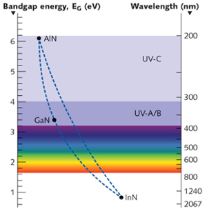
Nitride semiconductors are chosen because of their ability to form band gaps in the UV and visible region. Typical elements combined with nitrogen include Aluminum, Gallium and Indium. The image below shows the various wavelengths that can be emitted strongly by each compound.

Emission wavelengths for various Nitride semiconductors. Courtesy LaserFocusWorld.
Intermediate doping profiles can be obtained by varying the composition of elements. For example, visible to IR light can be obtained by varying the Indium composition in a GaN system. Similarly, varying the aluminum composition in GaN can make one get wavelengths in the UV region. While this seems easy in theory, doping elements are not as easy as compared to doping in a silicon crystal, as the quality of the film degrades. This is the reason indium doping for efficient green emission remains a challenge.
Manufacturing Techniques of Nitride Semiconductors
Nitride semiconductors were made possible with advances in deposition techniques. Deposition of films is done by metal-organic vapor phase epitaxy (MOVPE). In this technique, trimethyl compounds of aluminum, gallium and indium are introduced into the deposition chamber with ammonia for carrying nitrogen. Chemical reaction at the substrate causes the deposition of nitride films. By controlling the amount of each gas in the chamber and the deposition time, the film thickness and doping profile can readily be controlled.
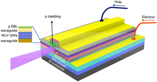
Deposition of GaN films were also explored in the industry before 1997, but none were able to overcome the principal problem of high defect density in GaN films. Nakamura’s group tackled this problem by introducing a buffer layer between the substrate and the nitride film to keep the defects manageable. The image below shows the nitride laser diode deposited on a silicon substrate, with a buffer layer in between.

Structure of Gallium Nitride based laser diode. Courtesy Semiconductor-Today.
Nitride semiconductors can also be made using quantum well structures to increase the conversion efficiency from electrical to light energy. Other substrates such as sapphire and zinc oxide have also been used instead of silicon as substrates for deposition. Commercial production of nitride lasers such as blue lasers are being made by companies such as TopGaN.
Applications
Nitride devices open up many applications because they allow engineering of relatively large band gaps by doping these materials. In photonics, these high bandgaps can be used to emit and detect light in the visible and UV region. They are more efficient than frequency doubling techniques, and enable reaching high powers through laser arrays. In electronics, the large bandgap makes them robust and helps withstand high temperatures and breakdown voltages. This makes them useful for high power electronics, electronics for military applications, robust detectors for UV light and nuclear reactors. Because of the wide range of applications, the market for nitride devices is forecasted to increase exponentially as shown in the image below.
Current and estimated market share of GaN device. Courtesy grandviewresearch.
Unfortunately factors such as the cost of production make nitride products less affordable compared with devices made from standing silicon doped semiconductors. However, with improvements in process efficiency and yield, these products can be seen to reduce cost in the future.
Fluorescence Spectroscopy
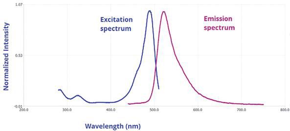
One exciting new application of nitride devices is their use in fluorescence spectroscopy for detecting molecules. Conventional diode lasers emitting light in the red to infrared region can be used for vibrational spectroscopy but not for electronic states. In order to probe electronic states, light in the visible and UV region is required. Fluorescence spectroscopy works by exiting molecules in the UV or visible region to force molecules to emit in the visible region. This is very attractive for visible detection of biological species by staining them with fluorescent molecules. Typically, part of the input excitation energy is converted into heat before the output emission occurs. The image below shows the spectrum of such a process.

Input and output spectra in Fluorescence spectroscopy. Image courtesy of Horiba Scientific.
Nitride lasers work well for fluorescence spectroscopy as they can excite molecules using visible and UV light. Moreover, high power nitride lasers can be used for multiphoton excitation spectroscopy of these molecules.
Future Applications
Nitride materials for photonics has challenges to be overcome to become a truly versatile technology in the visible and UV domains. For example, doping with Al and In are not as efficient in the UV and green region respectively thus making high power applications hard to achieve. This has also resulted in ‘green gap’ as efficient green light emission is hard to achieve. Advances in these fields with improved deposition techniques is foreseen for future players in the industry.
Did you like this article? If you did, subscribe and share!
