Particle accelerators can cut silicon. In general particle accelerators have had many applications for the field of particle research, physics, and have broadened our understanding of matter. On top of this, particle accelerators are a marvel of engineering. One of the latest uses sees extremely thin wafers of silicon cut using particle accelerators with no material loss! In this article we will discuss how this works and why this innovation is so interesting.
Today’s post is sponsored by Connet Lasers – a global leader in fiber laser technologies.
Understanding what we use silicon for
To begin appreciating this innovation we must begin with understanding how we use silicon. Processed silicon forms cylinders known as boules. Boules get cut into thin wafers which serve as the material basis in our electronics via transistors, computer chips, and solar panels. Silicon’s use as a semiconductor lends it to be one of our most valuable materials for creating transistors, which are the building blocks of digital memory in virtually all electronics. Due to these same properties silicon often make up an important layer in solar cells which build into full solar panels.

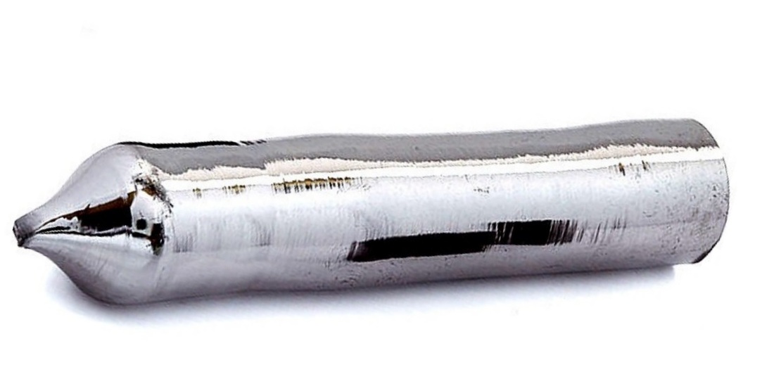
Silicon boule before being cut into wafer. It is a single crystal ingot of silicon with one continuous crystal structure Image courtesy of Chipsetc.com
These boules are a single crystal. That is to say they consist of silicon atoms in an arrangement which holds them together in a standard pattern throughout the entire crystal ingot. It is in this condition that they are then cut into wafers which follow the processes as we brought up earlier in this section.
Silicon wafers are processed by cutting boules into wafers which are the base for creating computer chips among other things. Image courtesy of fujitsu.com
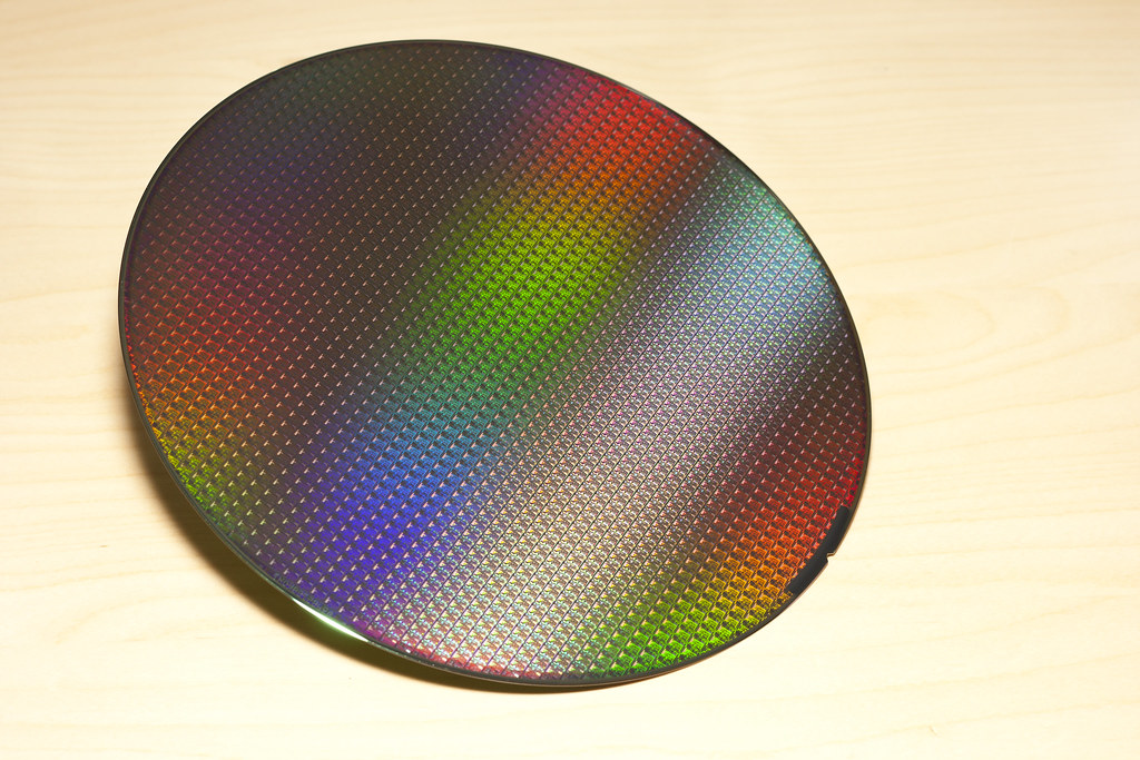
As shown in the image above, silicon is usually cut with a saw to create wafers, these wafers receive further treatments which refine them for their purposes from chips to full solar panels. The final result more often than not is a wafer of silicon you may see associated with electronics and computer parts.

An entire silicon wafer after being processed and prepared for use in creating more electronics.
How do particle accelerators cut silicon?
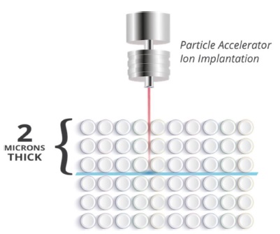
In the last decade, scientific and engineering communities alike have sought for innovative ways to process silicon. As an alternative to mechanical sawing, laser cutting, dicing and other technologies have proposed. One such interesting technology is the relatively low energy proton accelerators. In the proposed scheme, protons enter the lattice structure of the crystal and embed themselves between silicon atoms which applies more pressure on the surrounding atoms. These embedded protons are only able to penetrate the silicon to a depth determined by their energy. With this, the depth of the breaking becomes a function of the energy given to the photon and we can extract extremely thin wafers. Then, once heated the addition of the protons within the structure creates a line where the silicon will break first.

Demonstration of how layer of protons creates a line for the breaking of a single thin wafer. Image courtesy of sec.gov
Protons from a particle accelerator enter the crystal and create a line. when heated up this allows for the crystal to break across the line where the protons were absorbed in the crystal. Image courtesy of MinutePhysics
The application of this technology lies within the creation of thin wafers for solar cells. The idea is that the silicon crystal can be cut into incredibly thin wafer to use for the base construction of cheaper solar panels.
The benefits of using a particle accelerator to cut silicon
The main benefit with this method is having no material loss. As the image above shows the cutting is done between the molecules themselves within the crystal. This means that there is both a clean break and an incredibly smooth finish. With no material loss also comes a reduced need to re-crystalize and possibly re-purify any wasted material. This is in stark contrast with mechanical sawing which produces significant amount of both waste and scrap. When using a saw, there is inherent material loss due to the material removal mechanics of a saw. In principle the saws used to cut silicon are really removing a thin slice of material to separate one wafer slice from another. With the precision of penetration depth controlled by the proton energy comes control on the width of the wafers being cut. The size of these wafers cut by particle accelerators is in the range of a couple microns. Additionally, the thickness of the fine diamond saws lies in the range of 20~40 microns. Due to this, wafer production produces a significant amount of wasted silicon. Aside from this, a saw cannot reliably cut such thin wafers without occasionally breaking the slice.
The costs of using a particle accelerator to cut silicon
The biggest issue with this method is that particle accelerators are an expensive piece of equipment to produce and use. This makes the cost of initial investments extremely high. However this method has been used with a particle accelerator co-developed by Rayton Solar Inc. (a solar panel company) and Phoenix Nuclear Labs LLC at Phoenix Laboratories. This goes to show that co-development of more particle accelerators subsidizes the startup cost. Nonetheless the cost of a small particle accelerator still lies in the range of a couple billion dollars.
The upside to this process is a silicon wafer that as shown below could be about 25% cheaper than those produced by other methods, with additional savings thanks to not wasting any material when cutting. The advantages of this method only outweigh the costs after producing extremely large volumes due to the expensive equipment needed. It may be for these reasons that solar panels are not created this way today. This is easy to speculate since the method has existed since as far back as 2017 and the method clearly has not taken off.
Rayton published a comparison of how much the same kind of Gallium Arsenide silicon wafer costs to produce. image courtesy of Sec.gov
Conclusion
The prospect of cutting silicon with particle accelerators feels as though it is straight out of a science fiction. Yet it is a very real process that can create extremely thin wafers. The technology/mechanisms that allow for this process to exist are fascinating due to their intelligent and creative nature. As it stands, this process remains uncommon and virtually unknown. This being the case it is still possible for future innovations to require approximately 3 micron thick silicon wafers. Should that day ever come, the process may increase in use and popularity. Until then it is very fascinating to know we have developed a process to have a particle accelerator cut silicon.
