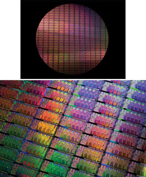
If you have ever thought about the microchips in your phone or wondered why the recent chip shortage is so important, keep reading! The answer starts with lithography, or more specifically photolithography. Photolithography has contributed to keeping Moore’s Law alive and has led major advances in creating microchips on silicon wafers.

Image of computer chips on a silicon wafer, courtesy of Photonics Media.
What is Lithography?
Lithography is derived from Ancient Greek lithos meaning “stone” and graphein meaning “to write,” it is a method of printing that uses the immiscibility of oil and water. German author and actor Alois Senefelder invented lithography in 1796. Creating maps and music sheets were the primary uses for lithography at that time. Since then, this printing method has been used to create art and book printing.
Of course, since 1796 there have been endless technological advances, so art and producing paper prints is no longer the main use for lithography. Modern lithography has advanced to four main types: optical lithography (photolithography), electron beam lithography, x-ray lithography, and ion beam lithography. Today, production of semiconductor chips used in all sorts of electronic devices such as phones, computers, and care is the most notable use of photolithography.
What is Photolithography?
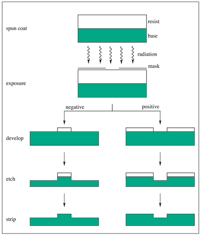
Photolithography is a general term for the process of using light to etch onto substrates like silicon wafers. The process is as follows: the substrate is coated with a thin film of a light-sensitive chemical referred to as photoresist. Then an optical mask, or “reticle,” is placed on top of the photoresist. Next, the light source is shined onto the reticle which transfers the design onto the wafer. There are two types of photoresists, positive and negative. To illustrate, negative photoresist masks the desired section resulting in an elevation. Positive masks the larger areas that we want to keep resulting in a groove. The masked area is what remains after the etching occurs. Typically, wavelengths in the ultraviolet and infrared spectrums are used for photolithography. A common use for this process is producing computer chips. In fact, hundreds of microchips can be made on a single silicon wafer.

Image depicting the photolithography process with negative photoresist on the left and positive on the right. Courtesy of Millipore Sigma.
Why is Photolithography Important?
In 1965 Gordon Moore, one of the founders of Intel, wrote an article for an electronics magazine. In this article he observed that the number of components on a silicon chip was roughly doubling each year. Moore’s law is his prediction that this trend would continue. This law has roughly stayed on track over the years due to manufacturing breakthroughs and innovative chip designs.
Photolithography is most used for chip productions. The features on a chip can be produced on the scale of nanometers when using optical lithography. Smaller features on a chip mean that more components can fit within the same space. This is a large contributing factor to Moore’s Law still holding true.
Latest Technology for Photolithography
In the late 1990’s there was a proposal to use extreme ultraviolet light (EUV) for photolithography. The company ASML is a leading manufacturer of the machines that will produce the chips, created using photolithography. ASML is the only company that has been making considerable progressto create EUV capable devices. These machines are quite costly at $150 million, so only a few top chip manufacturers like Intel, TSMC, and Samsung can afford them. EUV uses a wavelength of 13.5nm, and must operate in a high-vacuum chamber. It is these machines that the world is waiting for in high volume manufacturing to accelerate the production of smaller integrated circuits and help reduce the recent chip shortage and to get back on track.
What is EUV?

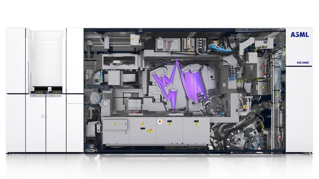
A look inside ASML’s EUV lithography machine. Image courtesy of ASML.
ASML explains how the extreme ultraviolet light is generated within these systems. A CO2 laser fires two separate laser pulses at a droplet of tin that is moving quickly. The tin droplet vaporizes and that makes EUV light through electron recombination processes in the plasma which contains highly ionized tin. This process is done up to 50,000 times a second and several mirrors guide the EUV light to the wafer. The wafer stage places the wafer within a quarter of a nanometer under the light for each exposure, constantly checking and adjusting. Read more about the process of obtaining and focusing EUV light for lithography in this article.
These new EUV lithography machines are more precise than anything created previously which allows for smaller components on chips. ASML is able to create smaller, more precise features on the chips they make by using multiple mirrors to shrink the beam as explained above. Machines like ASML’s EUV lithography machine are what will keep Moore’s Law “alive.” Of course, previously the EUV machines were the next thing. Being able to create and use 13.5 nm light in this system was a groundbreaking feat.
What is Next?
Now ASML has been distributing EUV systems for a couple of years. Next, they are working on new “High NA” EUV, while they continue to produce the previous EUV devices. NA stands for numerical aperture which is related to the image resolution. The NA of the system combined with the wavelength used determines the size of the smallest printable feature. ASML and Intel are collaborating on this work ASML making the system and manufacturing expected to start in 2025 for Intel. The new machines will improve lithography with reduced device complexity, cost, cycle time, and energy. The high NA systems offer a 0.55 NA, an increase from 0.33 on the previous EUV systems. This will provide higher resolution for even smaller features.
This post was brought to you by Zolix Instruments - supplier of scientific instruments and analytical solutions for material science and other applications

Thanks for helping me understand that photolithography would be used for chip production which would be made on the scale of nanometers with the optical process. I can imagine how there should be parts and processes that are used and done right to ensure that they work according to what they are for. I wonder what is the best use for Ultratech Titan and other parts when there is a need for replacements.