Why Measuring Temperatures at Micro-Scale is so Difficult?
Scaling temperature measurement techniques from the macro- to micro-scale proves quite difficult due to the evasiveness of temperature sensing technologies. Contact measurements like scanning thermal microscopy or Seebeck-effect based thermocouples suffer from errors arising from transducing the thermal signal to an electronic one or thermal contact resistance skewing the actual temperature measurement. While non-contact techniques such as thermoreflectance or prototypical infrared cameras circumvent the above problems, they lack the spatial resolution and only provide bulk temperatures. Raman thermometry – a fundamentally different method of measuring local temperatures – offers non-invasive probing of temperatures at microscopic scale. The application of Raman spectroscopy to measure local temperatures has gained attraction in the semiconductor, polymer, battery or life sciences fields. In today’s post we will discuss what Raman Thermometry is, how it works and look into some applications.
From Spectroscopy to Raman Thermometry
Raman Spectroscopy and Phonons
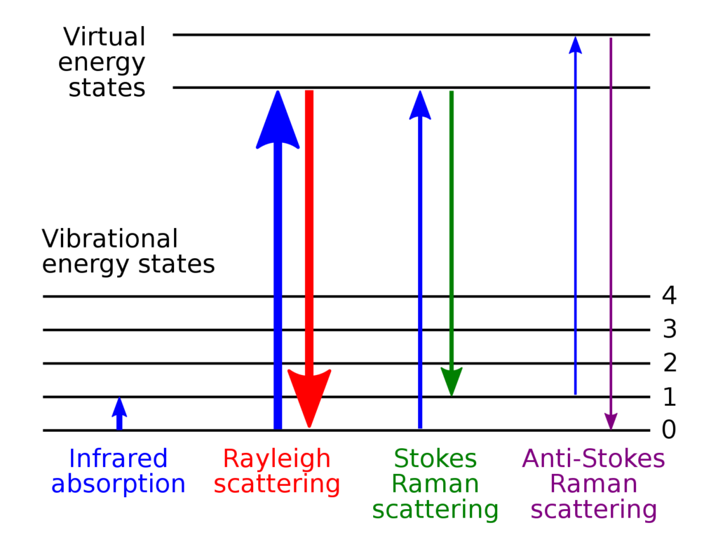
The basics of Raman spectroscopy relies on the concept of Raman scattering. Raman scattering occurs when laser light interacts with vibrations – whether they be molecular or atomic in a crystal (i.e. phonons). Through this interaction the energy of the photons of a laser can be lowered or elevated in energy, referred to as Stokes and anti-Stokes scattering, respectively. In a typical experimental setup the material is heated or cooled, and a beam is focused on the sample to probe these vibrations. The laser’s frequency spectrum is altered after it interacts with the material, which can be deciphered by monochromatic spectrometers.
Despite its origins in identifying molecules, Raman scattering has been extensively used to study solid crystals. However, to successfully harness this methodology for solids, the material needs to exhibit a change of polarizability as its atoms undergo vibration, in order for it to be able to interact with the probing laser beam. In other words, the vibration of a molecule or crystal has to induce a dipole moment. To identify if such vibrations are Raman active – as in identifiable by a laser beam – group theory provides a theoretical basis on what symmetries allow for induced dipole moments. Photons interact with particular phonon groups in the crystal which abide by the same polarization rules as molecules.
These phonon vibrational frequencies are often much lower than those of the C-H, H-O, C-O, etc. vibrational frequencies. Thus the elastically scattered light – Rayleigh scattered light – can conceal the inelastic light. So a special type of narrow-band rejection filters called Notch Filters are used to reject the Rayleigh light to allow the monochromator and CCD to measure the (anti-) Stokes light.
Phonons can be thought of as the quantization of the crystal lattice and therefore responsible to transporting and storing heat. So directly probing these phonons via Raman spectroscopy helps elucidate how energy is converted in a lattice. Emerging opto-electronic devices heavily rely on the conversion of electrons to photons, with phonon production (heat generation) being an undesirable side-effect. Understanding how materials heat up by electric or optical means is necessary for nano-scale device design, which is where Raman spectroscopy may aid.
Extraction of Local Temperatures
Phonons in crystals are classified into two groups – acoustic or optical. Acoustic phonons span multiple unit cells in a crystal. They can be thought of long wavelength vibrations in the crystal. Optical phonons correspond to vibrations within a unit cell, which are much shorter in wavelength so higher in frequency. Optical phonons are on the same energy level as visible light photons, hence the name and inclination to couple. These optical phonons are what induce the electric dipoles that allows or enables Raman scattering. Acoustic phonons lack the ability to produce such dipoles.
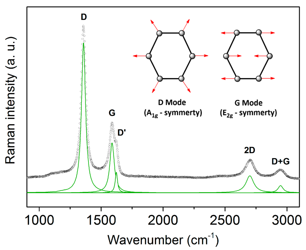
The measured Raman line shape of an optical phonon is Lorentzian, of which the three parameters correspond to phonon properties: Intensity is the population of phonons, linewidth is the lifetime, and peak position is the vibrational frequency. The below image shows an example of Raman spectra of 2D Graphite, or the well-known Graphene. The raw data (black) is fitted with Lorentzian line shapes corresponding to the D and G phonon modes, shown in the inset. Peak position and linewidth can readily be calibrated by using a first or second order empirical relationship with a macroscale temperature. The Raman technique can then be applied to determine sub-micron local temperatures in heterogeneous samples without thermal noise.
Raman thermometry is unique in that it directly probes phonon populations, which can be “converted” to a temperature. An expression for this temperature can be derived from quantum statistics and measurement of the anti-Stokes and Stoke peak intensities:
This temperature can be used to represent the macroscopic temperature, but it inherently reflects the temperature or “population” of the phonon group it measurements. If multiple phonon temperatures are measured, Raman thermometry allows for exploration of which phonon groups are more relevant in excited materials or microdevices. This is critical in designing the next generation of photovoltaics, electronics, LEDs, etc., where thermal management is a key issue.
Applications of Raman Thermometry
Raman thermometry is heavily utilized in the semiconductor and microelectronic industries. The miniaturization of electronics are hindered by inefficiencies in energy carrier conversions, more specifically in either electron-electron or electron-photon processes. Raman thermometry allows researchers to explore how phonons are generated and find ways to mitigate heat effects. For example, hot spots often occur in transistors which can be detrimental to device performance. Raman thermometry allows for temperature mapping in an non-invasive manner to aid in thermal management decisions when constructing microelectronic devices.
Furthermore, Raman thermometry is powerful in correctly analyzing emerging material properties. Because it is a non-contact measurement technique, it does not introduce complexities arising from interfacial effects that exist in full contact measurement techniques. The latter can skew measurements because interfaces add electronic and heat resistances to the transducing device, i.e. thermocouple. This is especially important in 2D materials with a large ratio of surface area to volume. Raman thermometry allows for the extraction of properties like thermal conductivity and diffusivity with relatively low error. It has been useful in proving the high thermal conductivity of graphene and other interesting transport properties of other 2D materials like transition metal dichalcogenides (TMDs).
Time-Resolved Raman Measurements
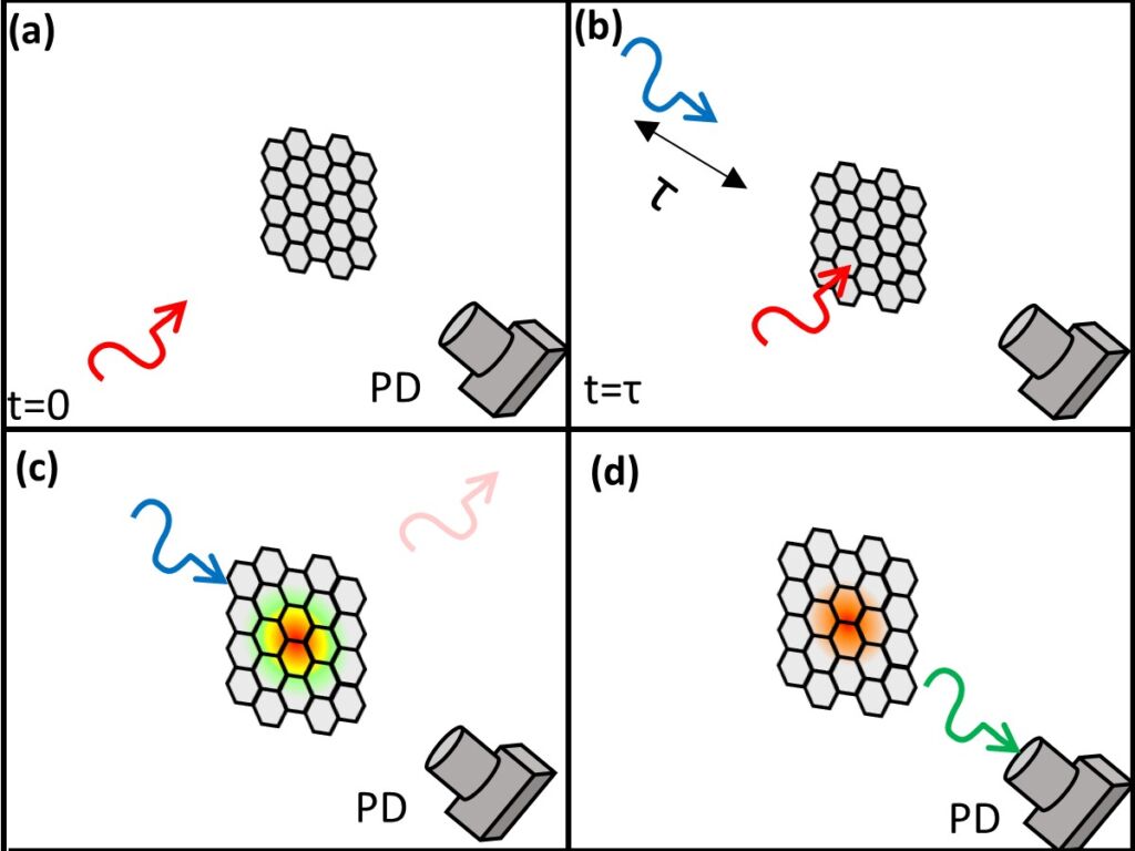
Raman thermometry can also be extended to provide temporal information of the system of interest. Examples of using anti-Stokes Raman spectroscopy include determining flame temperatures and thermal properties of materials. Because a Raman spectroscope can directly probe specific phonon temperatures, one can use time-resolved Raman spectroscopy to explore how different phonons couple to timed excitations. For example, using pump-probe techniques it is possible to excite electrons and then measure which phonon groups directly couple to these excited electrons. These experimental setups often include optical delay lines which control the delay between the laser beam exciting the sample and the probe beam collecting information. The optical delay line allows scanning the temporal distance between the pump and probe excitation pulses. By probing the sample at different time delays upon excitation the measurements allow reconstructing the temporal dynamics of the excited state of the system.
A very simple schematic representation of such an experiment is shown in the diagram above: in (a), the pump beam is sent to the sample. After a time delay, the probe beam is sent (b). In (c), the pump beam heats the sample while the probe beam passes though, after which the probe beam enters the photo detector for analysis. Understanding the time-resolved interactions of electrons and phonons can help explain joule heating in transistors, extending photovoltaic efficiency, and a myriad of other opto-electronic devices.
Conclusion
Raman spectroscopy can be extended for temperature sensing to a technique called Raman thermometry. The line shapes provide thermal information about the heated material or device. This can either be a local effective temperature of the probing beam or the temperature of an individual phonon group. This better educates engineers of the exact relevance of energy carriers in microelectronics, whether that’s an electric carrier or a heat energy carrier. Furthermore, extracting material properties can be done with relative ease using Raman thermometry. Any Raman techniques can be extended to time-resolved measurements, which can provide additional information on the thermalization times of these excited energy carriers. Raman thermometry is proving to be more popular in the thermal and microelectronics communities due to its ease of use and evasiveness of the sample of interest.
Today’s blog post is sponsored by Zolix Instruments – professional manufacturer of scientific instruments and analytical solutions for material science and other applications. You can check out their Raman Spectrometers here.


