Sub-nanometer imaging is desired over a range of different fields with uses from profiling thin films to investigating biological materials. In this blog post we will explore some of the methods for producing sub-nanometer images. It is noteworthy that many of the methods listed below are techniques using either some form of spectroscopy, microscopy, or both.
Atomic Force Microscopy (AFM)
Atomic Force Microscopy is often implemented for imaging biological systems/molecules at high resolution and has even been used to measure forces between such molecules. While it is used heavily in biologically related applications, AFM is very versatile. Imaging materials such as glasses and polymers is also possible with AFM. This is an improvement upon scanning tunneling microscopy (STM), the precursor to AFM, which could only scan conductive materials or semiconductors.
AFM works by using a cantilever whose tip is raster-scanned over a surface. Typically, the surface must either be in air, a vacuum, or a liquid. When the tip is scanned over the surface, the tip’s interatomic forces interact with the sample in question. From the feedback from the tip and the deflection of the cantilever, a topographical image can be reconstructed. Some AFM systems use a laser whose reflection is then deflected onto a detector to scan the sample/material.
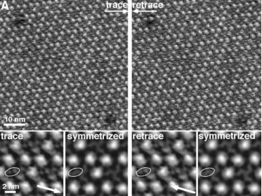
A group from the University of Basel in Switzerland was able to image biological specimens (proteins) at the sub-nanometer level. The biological samples were prepared by being diluted in a buffer solution. They found that different types of electrolytic concentrations used for this buffer solution produced different effects on the resulting images. The charge interactions rely heavily on the charge of the AFM tip and the sample. Depending on the buffer solution used, different forces were applied to the AFM tip. The best images were produced when the sample was under the most electrostatically balanced conditions. The smallest resolvable and reproducible details imaged had a width of 0.6 nm.

Some of the sub-nanometer resolution images of a membrane produced using AFM. Courtesy of Biophysical Journal
Electron Energy Loss Spectroscopy (EELS)
With this method of sub-nanometer imaging, particles of a sample are hit with electrons which excite the sample. The electrons that are elastically scattered (i.e. there is no change in the electron’s energy) from the sample are detected and used to create an image of the sample. A ratio is then taken from the amount of scattered, detected electrons to the to total amount of electrons from which an “electron energy-loss probability” can be mapped for every beam position. EELS is projected to be a critical method for identifying inconsistencies in structural changes in nanomaterials.
Photoluminescence for Sub-Nanometer Imaging
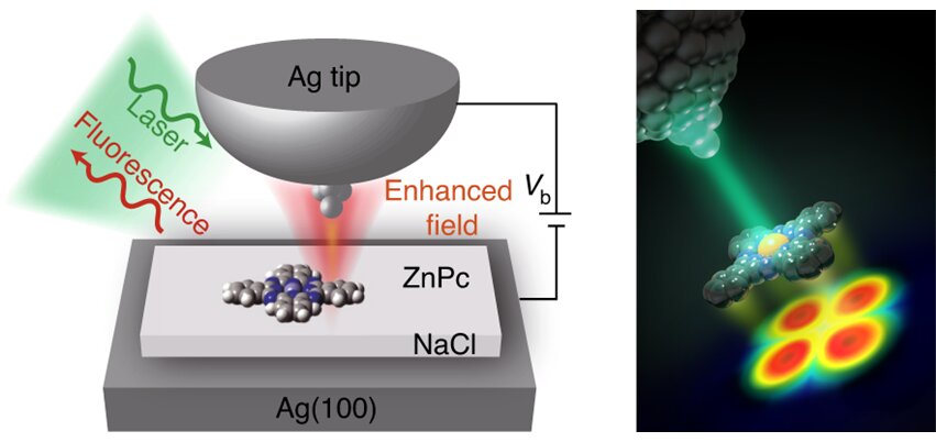
A group out of the University of Science and Technology of China is the first to have achieved a spatial resolution of approximately 8 angstroms using photoluminescence imaging. Their work was published in Nature Photonics in early August. This is an improvement upon the previously attained resolution of 8 nm. They were able to avoid the fluorescence quenching which was one of the keys to their imaging success. Fluorescence quenching describes anything that may decrease a sample’s fluorescence intensity. Molecular interactions can cause quenching. To avoid quenching, the team modified “the structure of the probe and the electronic state of the molecules in the nanocavity”.

A depiction of the setup used for sub-nanometer imaging using photoluminescence. Courtesy of phys.org
An image describing a visualization of the setup is included above. The group decided to use a silver-tipped probe. They matched the “nanocavity plasmon resonance with the effective energy of the incident laser and molecular luminescence”.
Simulations suggested that the structure of the probe’s tip and the resonance matching would create an electromagnetic field that would cause the localized photon density of states to increase. This would disallow quenching to occur and open the door for sub-nanometer imaging. This was confirmed in practice when the team discovered that even with the probe within a single nanometer of the molecule the intensity of the photoluminescence still increased with no quenching effects. This synergistic effect between the intensity and the absence of quenching provided the opening for sub-nanometer imaging.
Terahertz Sub-Nanometer Imaging
This method is be desirable because it is a way of performing sub-surface imaging that is both non-contact and non-destructive with respect to the sample. For this technique, a continuous wave (CW) terahertz energy source is delivered using a multimode fiber and coupled with both a spectrometer and nanoscanner. A terahertz camera produces an intensity distribution of the beam. The beam is focused onto the sample wafer and detected. Using the nanoscanner and image reconstruction techniques, a sub-nanometer, high resolution image can be created.
Scanning Tunneling Microscope with Tip-Enhanced Raman Spectroscopy (STM TERS)
The same group out of the University of Science and Technology of China mentioned in the Photoluminescence section was also successful at obtaining sub-nanometer information using Tip-Enhanced Raman Spectroscopy (TERS) controlled by a custom-made “low-temperature ultrahigh-vacuum” plasmon-enhanced scanning tunneling microscope (STM). The STM was kept at approximately 80 K and a pressure of approximately 1×10⁻¹⁰ Torr.
The samples to be imaged were two different types of porphyrin molecules that were thermally sublimed onto a silver substrate. Both the substrate material and the scanning tip were made of silver, as silver provides a strong plasmonic enhancement. When scanning the samples, the acquisition time was 1 second for each pixel. Previously, just using TERS it was difficult to obtain good image quality due to a low SNR relating to the necessary acquisition time and thermal drifting affecting the system’s stability.
After the scanning was complete, further multivariate analysis was necessary. Instead of just taking information from single peaks in the data, they performed analysis over the entire spectrum. This analysis mapped the chemical makeup of the porphyrin molecules and their spatial distribution, thus making it possible to resolve features at the sub-nanometer level.
Conclusion
There are clearly several sub-nanometer imaging techniques in existence that produce practical and valuable insights, but it would not be unreasonable to expect further development yielding better resolution and faster imaging speed.
This post was sponsored by DataRay Inc. – world leader in laser beam profiling solutions.
