Introduction to Superconductors (Traditional)
Superconductivity was first discovered in 1911 by Heike Kamerlingh Onnes when he found Mercury to have an abrupt drop in electrical resistance at a temperature of around 4.2K. Superconductors can be defined simply as a class of materials that have zero electrical resistance, and infinite conductance at or below a certain temperature, called the critical temperature and below their critical field. They are characterized by the fact that they are filled with Cooper pairs which creates a gap (band gap) in energy between the ground state energy and the first excited state. Electrons under this band gap are in the superconducting phase and the electrons above are normal (in resistive state) electrons. It is an interesting subject because these materials allow current to persist in them for times longer than the age of the universe without external power sources. Photonics applications can take advantage of Superconductor transition properties that rely on temperature and electrical current applied. Superconductor Spectroscopy applications include Photon detectors for X-rays used in medical devices and astronomy missions.
Spectroscopy Applications with Superconductors
Superconductor Spectroscopy Device 1: Optical Photon Detectors
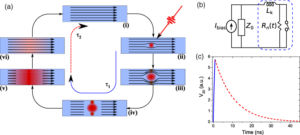
Operation: The Superconducting nanowire single photon detector (SSPD/SNSPD) device consists of a nanowire made of superconducting material, kept in its superconducting state (below critical temperature, and magnetic field applied). Small sections on the microscopic level in the wire absorb incident photons. This absorbed energy disturbs the Cooper pairing that causes Superconductivity in that region. Thus, some finite resistivity forms which repels Superconducting currents from the section. Because of this, current/ magnetic field will become more dense in the outer regions of the wire. As a result, this breaks superconductivity in the whole width of the wire. The resulting resistivity of the wire blocks off superconducting currents flowing through the other sections of wire. The increase in resistance also creates a voltage pulse (due to Ohm’s law, V=IR). These changes indicate that a photon has been absorbed by the device. In order to reuse the device, joule heating and a bias current is added to restore the section of wire back to its original superconducting state.
Design: The detection area can be maximized through design of the materials used. Additionally, with different types of superconductors, these devices can narrow down the search for photons with specific frequencies (e.g. infrared photons are in 300 GHz – 430 THz range, which can bridge the gap energy for superconducting NbN).

Diagram of detection cycle in superconducting nanowire single-photon detector (SNSPD). Courtesy of iopscience
Superconductor Spectroscopy Device 2: Transition-Edge Sensors (TES)
Usage: A similar application to SSPDS is in transition-edge sensors (TES). TES are microcalorimeters/bolometers widely used in photon and particle/ infrared spectroscopy as in X-rays. A property of TES is that lower temperatures equate to a higher energy resolution (current aims by NASA: 4 meV or better). High energy resolution is important for applications in imaging spectrometers. As a result, these devices must be operated in cryogenic temperatures. As SSPDS, they consist of an absorber (of energy), thermometer, and a cooling component to return the device to its original state for reuse. Efforts are being made to use large array TES for future purposes in X-Ray astronomy missions.
Operation: First a bias current is applied to thin films of superconductors with clean transitions (Type I). During the process, the surrounding temperature must be in the transition region of normal to superconducting states (around critical temperature). Next, incident photons/ particles will give just enough energy (on order of mK) to heat up the device to break superconductivity. Subsequently, a current change occurs which is finally measured by a SQUID ammeter in the thermometer.
Superconductor Spectroscopy Device 3: Multipixel TES Layouts
Higher spectral resolution (i.e. can pinpoint location better) and higher energy efficiency (with vast energy range 0.1-10keV) is possible through Multipixel TES layouts. What these look like are arrays with multiple pixels of TES devices with their absorbers. These devices can be used to help detect and extract information from black holes, galaxy clusters, and the evolution of our galaxy. Additionally, Multipixel TES layouts were to be included in plans for the international x-ray observatory (IXO). (IXO was canceled in 2012 due to increasing costs.)
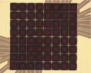
Current arrays built have 95% X-ray stopping efficiency and at 10 keV. With larger arrays on the scale of tens of thousands, we can aim for very precise energy resolution (4 eV or better). However, this would result in a very complicated mechanical structure, which can be resolved in a similar arrangement called a “hydra.”

8 x 8 array of TES microcalorimeters with 95% X-ray stopping efficiency at 10 keV. Each Pixel is 250 μm on a side and has a Mo/Au TES and a Bi/Cu absorber.
Courtesy of NASA
Hydras
Introduction and Considerations:
Hydras consist of arrays of multiple arrangements with several absorbers linked to one TES device. Hydras have more simple electrical connections and readout components compared to single celled pixel arrays. As a result, they are more efficient and easier to build. However, they do falter in the energy resolution at which they can read at and the count rate compared to single cell arrangements.
Design:
The connections between the absorber and the TES each have a unique thermal conductance. As a result, this allows people to match the absorbed energy signals with the pixel it came from. Additionally, this layout includes an electrical bias circuit to help return the device to the superconducting state.
Thermal model of multiabsorber TES with electrical bias circuit diagram.
Courtesy of SPIE
Superconductor Spectroscopy Device 4: Josephson Junctions & Applications
Introduction: As mentioned in the introduction of this article, currents can persist in Superconductors indefinitely due to their nonexistent electrical resistance (in Josephson Junctions this is called the Josephson effect). Devices can take advantage of this property, in what is known as a Josephson Junction. This device consists two or more Superconductors connected by insulators in between each. The next section will talk about research done using high temperature Cuprate Superconductors to create Josephson Junctions.
High Temperature Cuprate Superconductors
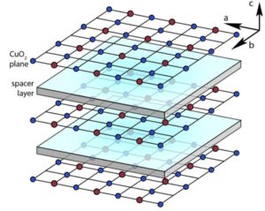
History of High Tc Superconductors: High temperature Superconductors are slightly different from traditional Superconductors in the fact that their properties depend on the direction of their electron-electron interactions. Their critical temperatures are also typically much higher (over 30 K). The first High temperature Superconductors to be discovered were Cuprates, with YBCO and BSCCO being some of the most popular.

Layered Cu02 superconductor and insulator structure
Courtesy of Nature
Design & Usage: Josephson Junctions created with these Cuprate Superconductors are stacked in 2D layers with a superconductor-insulator-superconductor pattern. Due to the Josephson effect, frequency can be set with the bias voltage level. Josephson Junctions with Cuprate Superconductors are advantageous because they can produce narrow bandwidth THz signals. As a result, Superconductor spectroscopy devices are used in imaging, medical diagnostics, and security applications.
